Monday, October 10, 2011

How to implement a generic ASIC Mix signal: An analog circuit for a glitch free Power-On-Reset signal for Digital block

Here are some implementation details related to the specification outlined in the other blog entry:Generic ASIC Mix signal specification: An analog circuit for a glitch free Power-On-Reset signal for Digital block ( referred as “Specification”).


One possible solution involves: RC parallel circuit and Common source stage with NMOS
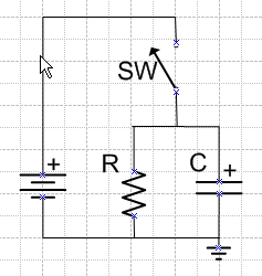
  • RC parallel circuit


Notice here that after closing the switch  VC is climbing immediately to VBAT while after opening the switch, capacitor is slowly discharging  trough resitor R.


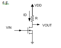
  • Common source stage with NMOS.


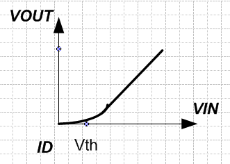
Here are some well known,  basic Voltages and Current dependencies of the circuit.

Without going to much details here is some basic explanation how basic Voltages and Current change in Common source stage with NMOS :

·         If VIN = 0, NMOS is not conducting so ID=0 and consequently  VOUT= VDD.
·         if VIN starts to increase voltage, ID starts to appear and increase in value too while VOUT falls in voltage because VOUT = VDD - ID*R.
·         if VIN  continue to grow it voltage,  at the point when VIN - Vth = VOUT, VOUT is getting closer  to 0V, and ID to its max. value ID=VDD/R


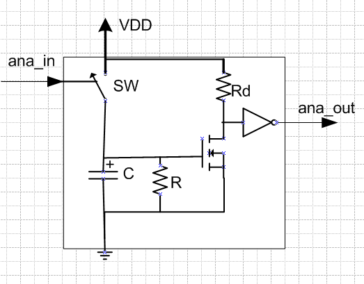
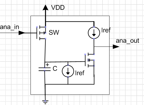
Finally here is an implementation hint for our analog circuit:


Here is an explanation what happens to ana_out voltage  when Switch (SW) is manipulated:

  • Lets assume at the beginning SW was closed for a reasonable long time so capacitor ( in the same time gate of NMOS) is for sure fully charged on VDD.

Consequently  NMOS is conducting with ID = I through Rd= max value of VDD/Rd so the input of inverter is 0 (VDD – IRd*Rd)  and  ana_out = 1       

  • Now lets open the SW: Capacitor is discharging with the the current through R  (this will take some time)
    • VC= Vgate, source voltage  is falling,IRd is falling too so  NMOS is  conducting in linear mode and  input of inverter voltage is rising.
    • While C is discharging, VC=Vgate, source voltage  is getting smaller, IRd is getting smaller too so at one point: VC-Vth= ana_out, and IRd is getting very close to 0.

At that moment  NMOS is  not conducting any more and input of inverter voltage becomes very close to VDD and ana_out = 0.  
  • Now lets close the SW:   Capacitor is charged immediately to VDD (Vgate, source = VDD immediately and NMOS starts conducting immediately in saturation mode with maximum current )  so input of inverter voltage goes immediately to 0V, and  ana_out = 1.


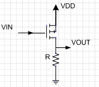
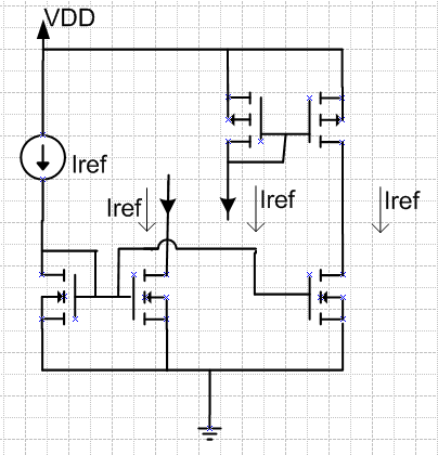
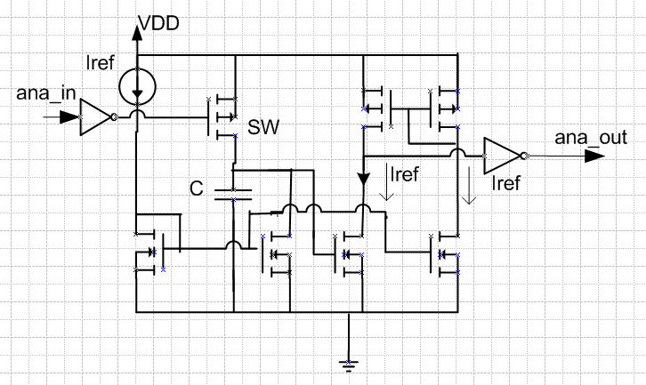
 We could improve  the design by replacing both resistors with reference current sources, mirrored and/or derived from a “ golden reference”. Also instead of switch we could use PMOS in common drain configuration (“source follower”).


  • Switch as PMOS source follower


  • Current sources mirrored from a “golden reference”


Final, more detailed schematic of the complete analog circuit:


© 2011 ASIC Stoic. All rights reserved  

Generic ASIC Mix signal specification: An analog circuit for a glitch free Power-On-Reset signal for Digital block

Digital block, in order to perform it s function as a part of an ASIC Mix signal design,  has always need a minimum two  input signals. One is clock and the other is Power-On-Reset signal (por).

por  can be implemented as Digital block power undervoltage signal. 


One possible implementation , related to the specification outlined here, is described  in the  blog entry:How to implement a generic ASIC Mix signal: An analog circuit for a glitch free Power-On-Reset signal for Digital block


When Digital block is not power-ed por keeps Digital block under reset (not functional). This make sense because if Digital block is not powered correctly it is not able to perform its function.  

por  is specified to be “active low” in other words when its value changes from 1 to 0 (”falling edge” of por ), Digital block will be reset-ed and kept under reset.
On the other hand when por is 1,  Digital block is functional.

Undervoltage detection filter time (t_v2_5_uv)


In designing analog circuit of por  it is important that por changes from 1 to 0 is glitch free.
When por changes from 1 to 0 and stay 0 during Undervoltage detection filter time (tv2_5_uv alredy described  in a previous blog entry.), only then Digital block should perform its reset.
On the other hand there is no need for glitch free signal when Digital block is getting out of POR reset(por changes from 0 to 1).

Assumption here is that  por already exists but is not glitch free, so that is an input (ana_inp) to the analog block specified here. And the output (ana_out) is por glitch free.


© 2011 ASIC Stoic. All rights reserved  

Thursday, October 6, 2011

Generic ASIC Mix signal specification: Powering of ASIC’s internal circuits, both analog and digital


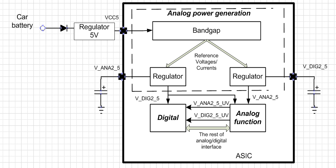
For the purpose of the ASIC’s internal powering, the specification is planning three ASIC pads:

  • one input external voltage power source 5V (VCC5)  and
  • two ports of internally generated and used  voltage powers 2.5V ( connected to capacitors to stabilise internal regulators)  
    • one powering analog circuits(V_ANA2_5) and
    • the other powering digital circuits(V_DIG2_5)  


Fig. 1 e.g. In automotive system it is possible to have car battery supplying external regulator 5V to supply power to VCC5 pad of the ASIC.

  • A note on micro-architecture choices made in the ASIC Mixed signal in Fig1

Assumption done here is that will be necessary to have two voltage regulators separated for powering analog and digital block. The reason  is that digital blocks tend to  produce a lot of noise on its power line. Each regulator  is receiving necessary reference voltages/currents from a bandgap. Also each regulator with need an external capacitance for stabilization.

  • Also there is a requirement to detect and report Undervoltage condition on both  V_ANA2_5 and  V_DIG2_5.

Maximum Rating

Maximum rating describes that our ASIC will not get damaged even if V_ANA2_5, V_DIG2_5  voltages goes to extremes: minimum -0.1 and maximum 3.5V.
Guaranty of Maximum Rating  is not guarantee that the ASIC would be operational  unless V_ANA2_5, V_DIG2_5 are in  a normal operational range.


Pad nameValue= Min, Max
V_ANA2_5, V_DIG2_5-0.1V, 3.5V


Normal operating conditions

Pad nameValue= Min, Typ,  Max
V_ANA2_5, V_DIG2_5            2V, 2.5V, 3V


Note: During normal operation for the purpose of the ASIC functionality here is specified that  ASIC will always produce voltages V_ANA2_5, V_DIG2_5 in the range of 2-3V, and typical or average value should be 2.5V.

Undervoltage condition


The ASIC should monitor and report Undervoltage condition on either one of voltage V_ANA2_5, V_DIG2_5.
In the case of Undervoltage condition on either one of V_ANA2_5, V_DIG2_5 , a register flag v2_5_uv is set  and accessible by MPU after power VCC5 is restored to the ASIC .
Once set, the register flag v2_5_uv stays 1 until there is MPU read. The read clears the flag.

Undervoltage  condition  (V_ANA2_5_uv, V_DIG2_5_uv) ,  and filter time (tV2_5_uv)

The V_ANA2_5_uv, V_DIG2_5_uv Undervoltage condition is detected ( and the register flag v2_5_uv is set ) if either one of V_ANA2_5_uv, V_DIG2_5_uv  voltage is LESS then  min=1.5V and max=2.1V ( typical value 1.7V ) , and this event is uninterrupted tV2_5_uv time, value 0.5us.


Parameter descriptionParameter SymbolValue: min, typ, max VComment
Undervoltage  fault
V_ANA2_5_uv, V_DIG2_5_uv1.5, 1.7, 2.1V


The V_ANA2_5_uv, V_DIG2_5_uv Undervoltage condition is considered not present any more if once detected,  both V_ANA2_5, V_DIG2_5  voltages is  MORE then V_ANA2_5_uv, V_DIG2_5_uv , and this event is uninterrupted tV2_5_uv, value 0.5us.

The time tV2_5_uv=0.5us of detection/cancellation of V_ANA2_5_uv, V_DIG2_5_uv Undervoltage condition  is called Undervoltage detection filter time.

Parameter descriptionParameter SymbolValue:typComment
Undervoltage detection filter time
V2_5_uv0.5usThe filter not possible to implement in digital block: digital power undervoltage is Power on Reset (POR) for digital block.
Please see blog post: How to implement a generic ASIC Mix signal: An analog circuit for a glitch free Power-On-Reset signal for Digital block

 
© 2011 ASIC Stoic. All rights reserved

Wednesday, October 5, 2011

How to implement an ASIC Mix signal for an Automotive application: ASIC's Supply Pin connected to a car battery

Here are some implementation details related to the specification outlined in the other blog entry:  ASIC Mix signal Specification: Automotive application: ASIC's Supply Pin connected to a car battery  ( reffered as “Specification”).


The implementation will be divided  on analog and digital part.

Analog part

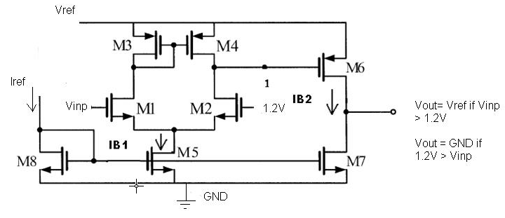
To monitor VBAT_uv or VBAT_ov we could use analog comparators. Here is an example of Unbuffered, Two-Stage CMOS Operational Amplifier that we could use an analog comparator.


In the Specification it was mentioned just VBat ( car battery voltage ) but to use the comparator we will need in the ASIC couple more reference voltages and currents.
  • a reference current Iref for a current mirror used in the comparator
  • a reference voltage Vref for alimentation of comparator transistors
  • a reference voltage 1.2V (used in voltage comparison). Here is an assumption made that the reference voltage 1.2V is a very stable voltage produced by  another analog circuit present in the ASIC:  e.g. bandgap.


Here is a hint how to use two instances of the comparator to produce VBAT_uv and VBAT_ov.

There is no need to detect VBAT_ov and VBAT_uv if a digital block of the ASIC Mix signal is under POR ( Power-On-Reset). VBAT_ov and VBAT_uv signals will exit analog block of the ASIC and enter the digital block, but if digital block is under reset,  the register flag vbat_ouv is not recorded anyway.

Digital part

Output of the analog part ( or its comparators ), VBAT_uv and VBAT_ov are inputs to digital part. A reasonable assumption here is that digital block is designed in synchronous manner meaning it is using only one clock (“clk”).
Before any use of non synchronous digital input signals VBAT_uv and VBAT_ov should be first resynchronized to the clock domain clk  using 2 Dff back to back.


t_VBAT_uv and  t_VBAT_ov are implemented also in digital block.


© 2011 ASIC Stoic. All rights reserved.

Wednesday, September 28, 2011

Verilog AMS: Code examples

Resistor, Capacitor, Inductor, RLC Circuit, Voltage and Current Sources, A Simple Circuit, Relay Digitally controlled Relay, Comparator, Simple 16-bit digital-to-analog converter model, Simple DAC ( digital input async. or no clock involved),DAC ( digital input async. or no clock involved, but  with reference voltage), Simple DAC ( digital input sync. on clock ), Analog tristate buffer, Voltage deadband amplifier, Hysteresis

Code examples

Resistor


In general, a resistor is a relationship between voltage and current, as in
v = ri
where v represents the voltage across the resistor, i represents the current through the
resistor and r is value of resistance of resistor.
v = V(p,n)
i = I(p,n)
v = ri

module resistor (p, n);
inout p, n;
electrical p, n;

parameter real R = 1.0;
analog
V(p,n) <+ R * I(p,n);
endmodule


Capacitor

A capacitor is a relationship between voltage and charge, as in where v represents the voltage across the capacitor, q represents the charge through the capacitor and c is capacitance of capacitor:

q = cv

Capacitors current  is related to its charge like this:
i = dq/dt

So for a linear capacitor, current is:

i = c dv/dt

which is encoded as a Verilog-A/MS contribution statement as
I(p,n) <+ c * ddt(V(p,n));


// Linear capacitor
module capacitor (p, n);
parameter real c=0; // capacitance (F)
inout p, n;
electrical p, n;
analog
I(p,n) <+ c * ddt(V(p,n));
endmodule

Inductor


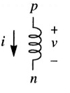
An inductor is a relationship between flux and current, where Φ represents the flux across the inductor, i represents the current through the inductor, and l is inductance of inductor.
Φ = li
flux is related to the voltage using:
v = dΦ/dt

the constitutive relation between inductance, voltage and current is:
v = l di /dt

// Linear inductor
module inductor(p, n);
parameter real I=0; // inductance (H)
inout p, n;
electrical p, n;
analog
V(p,n) <+ I * ddt(l(p,n));
endmodule


RLC Circuit
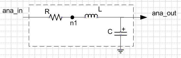


module rlc_behav(ana_in, ana_out) ;
inout ana_in, ana_out ;
electrical ana_in, ana_out ;

parameter real R=1, L=1, C=1 ;

electrical n1 ;

analog begin
V(ana_in, n1)    <+ R*I(ana_in, n1)        ;
V(n1, ana_out) <+ L*ddt(I(n1, ana_out)) ;
I(ana_out)        <+ C*ddt(V(ana_out))     ;
end

endmodule


Voltage and Current Sources

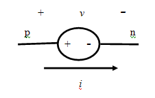
Constant voltage source


// DC voltage source
module vsrc (p, n);
parameter real dc=0; // dc voltage (V)
output p, n;
electrical p, n;
analog
V(p,n) <+ dc;
endmodule


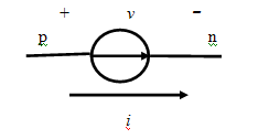
Constant current source

// DC current source
module isrc (p, n);
parameter real dc=0; // dc current (A)
output p, n;
electrical p, n;
analog
l(p,n) <+ dc;
endmodule

A Simple Circuit
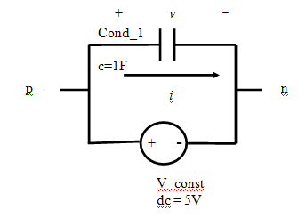


//A simple circuit
`include “V_const.vams”
`include “condensator.vams”
module smpl_ckt;
electrical p,n;

V_const        #(.dc(1)) V_const (p,n);
condensator #(.c(1F)) Cond-1  (p,n);
endmodule

Relay

A relay is a switch controlled by analog input (ana_inp),ideal in the sense that when the relay is closed ( ana_inp > treshold ), there is no voltage on its output (ana_out), and when it is open( ana_inp < treshold ) there is no current flowing though its ana_out output contact.
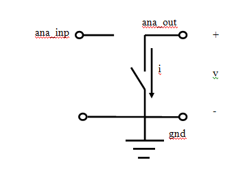

Verilog-A/MS model for an ideal relay.
// Ideal relay
`include “disciplines.vams”
module relay (ana_in, ana_out);
parameter real treshold =0;
output ana_out;
input ana_in;
electrical ana_out, ana_in;

ground gnd ;
analog begin
@(cross( V(ana_in) – treshold , 0 ))
;
if (V(ana_in) > thresh)
V(ana_out) <+ 0;
else
l(ana_out) <+ 0;
end
endmodule

Digitally controlled Relay


module switch (p, n, s);
input s;
output p, n;
logic s;
electrical p, n;
analog begin
if (s)
V(p, n) <+ 0.0;
else
l(p, n) <+ 0.0;
end
endmodule


Comparator

 
The input of this module is an analog input ( ana_inp ) and  the output is a logic signal ( dig_out ).

The output changes when the ana_inp crosses a certain voltage threshold, described as absolute value of parameter offset and parameter hysteresis. The parameter hysteresis provides the capability to add a hysteresis between the lower and the upper thresholds.

// Comparator with logic output
module comparator ( dig_out, ana_inp );
parameter real offset           = 0;
parameter real hysteresis = 0.0 from [0:inf);
inout ana_inp;
output dig_out;
electrical ana_inp;
logic dig_out;
reg dig_out;

ground gnd ;

parameter real thrlo = offset – 0.5*hyst; // Lower threshold voltage (V)
parameter real thrhi = offset + 0.5*hyst; // Upper threshold voltage (V)
always @(above(V(ana_inp) – thrhi))
dig_out = 1;
always @(above(thrlo – V(ana_inp)))
dig_out = 0;
endmodule


Simple 16-bit digital-to-analog converter


analog process is sensitive to the value of in at all times

Simple DAC ( digital input async. or no clock involved)

e.g. module dac (out, in);
parameter fullscale = 1.0;
input [15:0] in;
electrical out;
analog
V(out) <+ in * (fullscale/65536);
endmodule


Simple DAC ( digital input sync. on clock )


analog process is only sensitive to the value of in at the instant of a rising edge on clk


module dac (out, in, clk);
parameter fullscale = 1.0;
input [15:0] in;
input clk;
electrical out;
real smpld;
analog begin
@(posedge clk)
smpld = in * (fullscale/65536);
V(out) <+ smpld;
end
endmodule

Analog tristate buffer

This module evaluates the case statement whenever in changes and will set the local
variable value to 0 if in is 0 and to 1 if in is 1. Otherwise it leaves value unchanged.

Finally, it tests the value of in and if not z it drives V(out) with value, otherwise it
leaves out un-driven.

module buf3 (out, in);
input in;
output out;
electrical out;
real value;
analog begin
@(in)
case (in)
1'b0: value = 0;
1'b1: value = 1;
endcase
          
if (in !== 1'bz)
V(out) <+ value;
end
endmodule

Voltage deadband amplifier

If the input voltage is greater than vin_high or less than vin_low, the amplifier is active.
When the amplifier is active, the output is gain times the differential voltage between the input voltage and the edge of the deadband.

When the input is in the deadband between vin_low and
vin_high, the amplifier is quiescent and the output voltage is zero.


module vdba(in, out);
input in ;
output out ;
electrical in, out ;
parameter real vin_low = -2.0 ;
parameter real vin_high = 2.0 ;
parameter real gain = 1 from (0:inf) ;

analog begin
if (V(in) >= vin_high) begin
V(out) <+ gain*(V(in) - vin_high) ;
end
else if (V(in) <= vin_low) begin
  V(out) <+ gain*(V(in) - vin_low) ;
end
else begin
V(out) <+ 0 ;
     end
 end

endmodule


Hysteresis
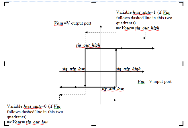


//--------------------
// hysteresis
//
// -  rectangular hysteresis
//

module hysteresis(Vin, Vout);
input Vin ;
output Vout;
electrical Vin, Vout;
parameter integer hyst_state_init=1;
parameter real Vout_high = 1 ;
parameter real Vout_low = -1;
parameter real Vout_high = 1 ;
parameter real Vout_low = -1;

  integer hyst_state;
  real    Vout_val;

  analog begin

     @ ( initial_step ) begin
      hyst_state = hyst_state_init;
     end

     @ (cross (V(Vin) - Vout_high,1) )
        if (hyst_state == 0)
           hyst_state = 1;

     @ (cross (V(Vin) - Vout_low,-1) )
        if (hyst_state == 1)
           hyst_state = 0;
 
     if (hyst_state == 1) begin
           Vout_val = Vout_high;
     end
     else begin
           Vout_val = Vout_low;
     end

     V(Vout) <+ transition (Vout_val);
  end
endmodule

© 2011 ASIC Stoic. All rights reserved.