Friday, December 6, 2019

Cadence Virtuoso CMOS Analog Design Basics in TSMC 22nm: a simple op-amp design with a High Swing Cascode current mirror- Part 2

Introduction


In this blog post we will finally design a simple opamp that will reuse our High Swing Cascode current mirror.


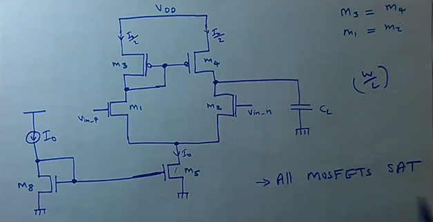
A design of a simple opamp is very well explained by  Hafeez KT, in his youtube lecture available online and here is a basic topology:
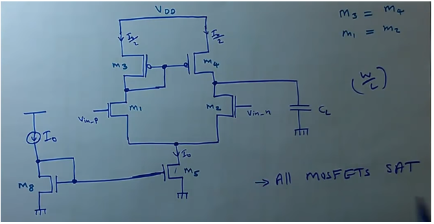
A summary of specification points that will be achieved in this opamp design:

  • our op amp has to drive capacitive load of C1 = 10pf with a 
  • Slew Ratio ( SR ) = 2V/second
  • Input Common Mode Range ( negative, minimum ):  ICMR- = 1.2V
    • Voltage on differential pair inputs should never be less than  1.2V
  • Input Common Mode Range ( positive, maximum  ): ICMR+ = 3.0V 
    • Voltage on differential pair inputs should never  not exceed 3.0V
  • Gain Bandwidth product ( GB ) > 3MHz)


Note* : L=1u for all transistors.


Calculation the value of current to be provided by M5 

A friendly reminder that our op amp has to have:
  • drive capacitive load of C1 = 10pf with a 
  • Slew Ratio ( SR ) = 2V/second
=>SR is rate of changing voltage across load capacitance C1
Q = C1 * V
dQ/dt = C1*dV/dt
I capacitance = C1*dV/dt
C1 is charging when differential pair branch M1/M3 is conducting ( consequently branch M4/M2 is not conducting ) with all the current I.
C1 is discharging when differential pair branch M4/M2 is conducting ( consequently branch M1/M3 is not conducting ) with all the current I.
Conclusion I of capacitance = I is:
=> I = C1*dV/dt
=> I = C1*SR
=> I = 10pF*2V/ u second = 20uA
=> I0 or ID5 = 20uA


Estimating ( by simulation )  p*Cox and n*Cox

for TSMC 22nm process PMOS and NMOS

transistor used

The technology that we are using here ( TSMC 22nm ) is new to me and I am
using pmos transistor pch_25od33_mac ( for M3/M4, pmos active load )  and I
don’t know its    


In general to calculate  W/L for M3/M4 we will use formula:
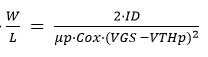
Then I setup a following simulation to find ( approx.) :
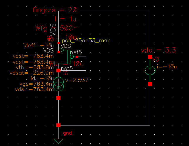
  • VDS = 3.3V
  • Idc = 10uA
  • W=10um
  •  L=1u
The DC simulation showed Vthp=603.8mV and Vgs=Vds=763.4mV
=> = 2*10uA/( ( 10um/1um) * (763.4mV - 603.8mV)^^2 ) 
=> = 7.85*( 10 ^^ -5 )
       Vth_p    = 603.8mV
Also I am using nmos transistor nch_25od33_mac ( for M1/M2, nmos differential pair  ) and here also I don’t know its n*Cox
Then I setup following simulation to find ( approx.) n*Cox
  • Idc = 10uA
  • W=10um
  •  L=1u
The DC simulation showed Vthn=672.2mV and Vgs=Vds=727.7mV
=> n*Cox= 2*10uA/( ( 10um/1um) * (727.7mV - 672.2mV)^^2 ) 
=> n*Cox= 649.2*( 10 ^^ -6 )
     Vth_n = 672mV 


Calculation of  W/L for M3/M4 ( pmos active load ) 

A friendly reminder of a points in specification:
  • Input Common Mode Range ( positive, maximum  ) , ICMR+ = 3.0V
    • Voltage on differential pair inputs should never  not exceed 3.0V


For calculation of  W/L for M3/M4 ( pmos active load ) let’s focus on highlighted transistors M1/M2:
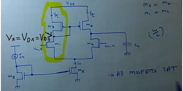


for transistor M0 to be in saturation VDS3 > VGS3 -Vth_p and ID1=ID3 = 10uA
if Vx = VD1 = VD3 and VDS1 > VGS1 - Vth_n => VD1 > VG1 - Vth_n
=> Vx > Vin_p -Vth_n
A friendly reminder: Vth_p    = 603.8mV and Vth_n = 672mV 


Maximum voltage on Vin_p = 3.0 V ( this is based on  ICMR+ = 3.0V ) and for Vin_p = 3.30V Vth-n=0.672

=>  Vx > 3.0V - 0.672 V = 2.328 V so we can adopt Vx  = VD1= VD0= 2.5V 
Since M0 is in saturation too, and VS0 = VDD :
=> VSD3 = VS3 -VD3 = VDD - 2.5 =3.3V -2.5  = 0.8V 
=> VDS0 =VGS0 = 0.8V 
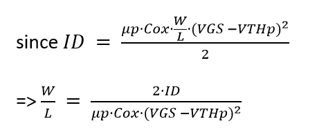
A friendly reminder: = 7.85*( 10 ^^ -5 )
=> W/L( PMOS M3) = 2*10uA/(79u*(0.8 -  0.604 )^^2 ) 


W/L( PMOS M3) =6.58 approx. 7


Calculation of  W/L for M1/M2 ( nmos diff. pair ) 


For calculation of  W/L for M1/M2 ( nmos differential pair ) let’s focus on highlighted transistors M4/M2:
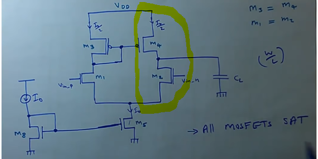

A friendly reminder of a couple specification points of our opamp::  
  • Gain Bandwidth product ( GB ) > 3MHz
  •  opamp is driving a capacitive load of 10pF


We will use formula GB=  DC gain * (first) pole
It can be proven that: 
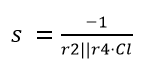
  • First pole:
=>


gm2= 3MHz*2*3.14*10pF= 188u
And because M2= M1 => gm2 = gm1

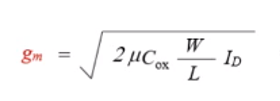
Finally to calculate M1,2 W/L we will use a formula gm=f(ID, W/L):


A friendly reminder:
  •  Vth_p    = 603.8mV and Vth_n = 672mV 
  • = 7.85*( 10 ^^ -5 )
  • n*Cox= 649.2*( 10 ^^ -6 )


=>  W/L ( for NMOS M1 and M2 ) = 2.74 approx. 3  


Fully transistor sized schematic ( but no current source implemented  yet )


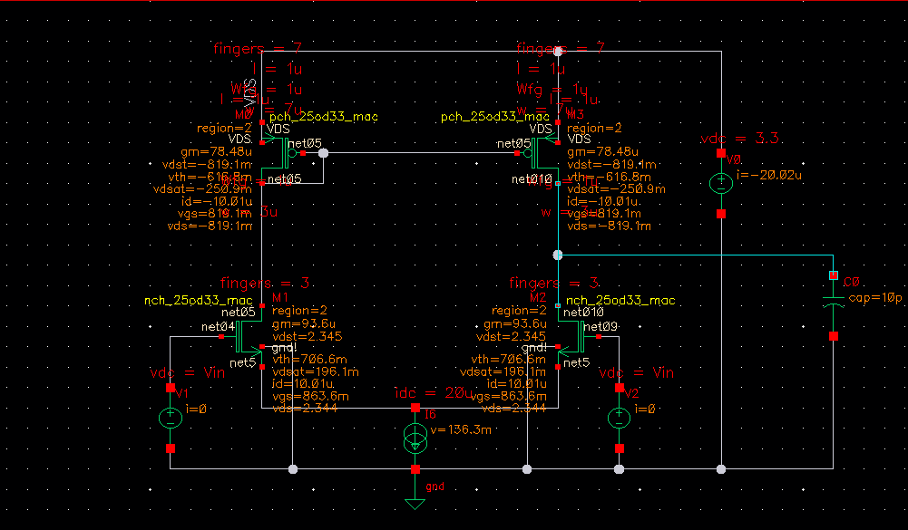
Finally our ( fully sized transistors )  schematic ( after DC simulation with annotated DC operating points ) including:
  • Vdd = 3.3V
  • Vin = 1V

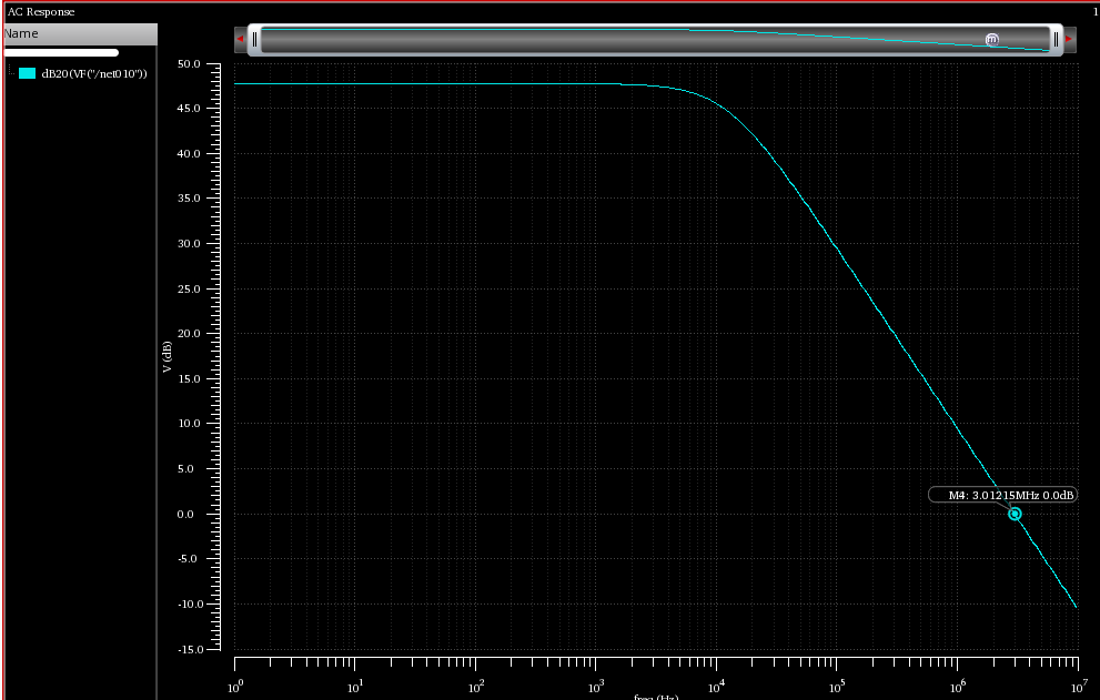
But did we achieve a point of the spec Gain Bandwidth product ( GB ) > 3MHz ?


A friendly reminder that Gain Bandwidth product is a frequency where 20log(output voltage/input voltage)=0dB and in our case Gain Bandwidth product is only 1.48MHz:
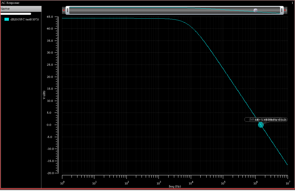


The lower than expected GB  is because a low value for gm of transistors
M1/M2 ( nmos differential pair ): gm1/2= 93.6u and to achieve
GB > 3MHz we calculated that gm1,2 should be gm1/2= 188u.
And to increase gm1,2 we need to further increase W1,2 to  W1,2=24u
to achieve gm1,2=188u :


Another useful check is to, in DC simulation,  “sweep” Vin from 0V to
3.3V ( VDD ) and to check that for  the range of valid Vin voltages (
ICMR- = 1.2V, ICMR+ = 3.0V )  all four transistors are in saturation:


Fully transistor sized schematic

Now we are replacing the ideal current source with High Swing Cascode
current mirror ( designed in the previous blog entry ):
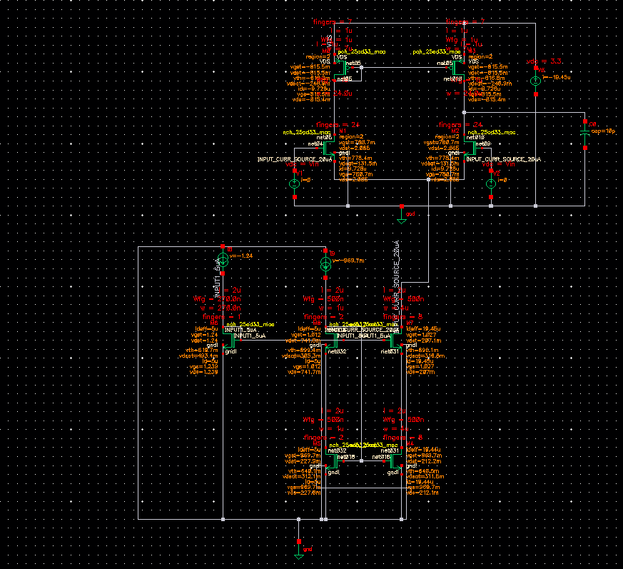

Again the  useful check to “sweep” Vin from 0V to 3.3V ( VDD ) in DC
simulation, and to verify  that for the range of valid Vin voltages ( ICMR-
= 1.2V, ICMR+ = 3.0V ) all four transistors of opamp core are in
saturation:
© 2019 ASIC Stoic. All rights reserved

Wednesday, October 30, 2019

Cadence Virtuoso CMOS Analog Design Basics in TSMC 22nm: a simple op-amp design with a High Swing Cascode current mirror

Cadence Virtuoso CMOS Analog Design Basics in  TSMC 22nm: a simple op-amp design with a High Swing Cascode current mirror


In the previous blog post “Cadence Virtuoso CMOS Analog Design Basics in  TSMC 22nm: “Constant gm bias circuit” with start-up and reduced sensitivity 
to changes in VDD” we needed to add an opamp.


A design of a simple opamp is very well explained by  Hafeez KT, in his youtube lecture available online and here is a basic topology:


But even the simplest opamp schematic would need a current mirror  ( NMOS transistors M5 and M8 ) provide necessary referent current Io .


In this blog post I  would like to explore  a High Swing Cascode current mirror a subject very well explained by prof. Nagendra Krishnapura  in his lectures
available online ( ee5320 2016 IIT Madras ).


For a “short channel” processes ( or other name is  a nanometer process ) such as TSMC 22nm , we should always use High Swing Cascode because 
ID5 is very dependant on VDS5 .


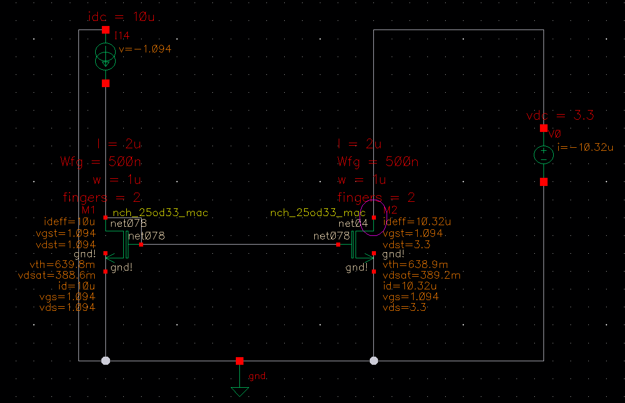
E.g. For VDS1=VDD = 3.3 ,  a change between VGS1=VGS2=1.094V to 3.6V is causing change of ID1 between: 10uA to 10.55uA. Expected value
ID2=ID1 = 10uA is true only if VDS1=VDS2=VGS1=VGS2=1.094V.


Variation of ID1 with a variation of VDD=VDS1 is no surprise because it can be proven that output resistance of M1 ( the resistance “seen” to the drain of M2 transistor) is 1/gds2 .
=> for a change of a delta Vout=VDS1 =>IDS1 changes to IDS1 + delta VDS1*gds2


Since for NMOS transistor M2 in saturation gm is:


=> there are two solutions to the problem of the small output resistance: 
  • somehow  increase the output resistance  or 
  • decrease gm ( or decrease W, or increase L or increase ID2=ID1=Io=10uA )


Decreasing gm is not really an option because our referent current is 10uA and we don’t want to “burn” more current/power. On the other hand  W/L of transistors M1 and M2 is
W/L=1u/2u, a reasonable small W and a reasonable big value of L.


=> The solution is an increase of output resistance.


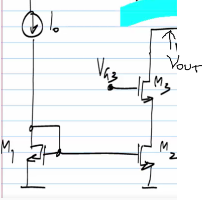
One of the solutions is to use a current buffer ( NMOS transistor M3 ). Current buffer would be a device that gives you the same current but a much higher output resistance.
  • A common gate stage is a current buffer ( cascoded transistor )


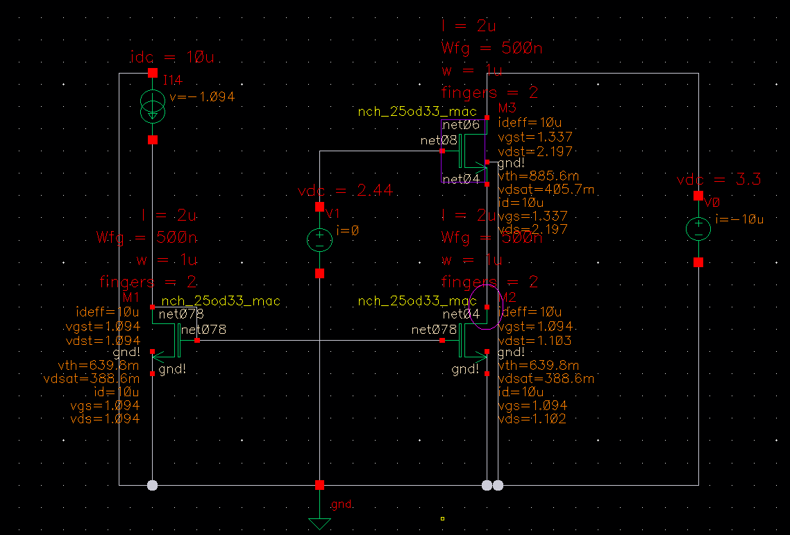
Biasing of NMOS transistor M3 could be found by “sweep” of V1= VG3 and at the same time observing ID1 to reach ID2=ID1=10uA.
  • The “sweep” value  of V1=VG3 to reach ID2=ID1=10uA is V1=VG3=2.441V which is in line with a following hand calculation:
    • Ideally M2 drain voltage should be VGS1 ( so M1 and M2 could be exactly the same and Id1 = Id2 = I0 ) and in reality  M2 drain voltage is
    • VG3 - VGS3 => ideally VGS1 = VG3 - VGS3 
    • => VG3 = VGS1 + VGS3
From simulation: VG3 =  VGS1(1.094V) + VGS3(1.337V) = 2.441V


Finally we achieved a much better stability of  IDS1 in relation to variation of VDD:
  • For a V0=Vout change from 1.18V to 3.6V, IDS1 change is from 9.99uA to 10uA:
    • Using cascoded transistor M3, we increased output resistance hence better result of the stable ID2=ID3=10uA with a variation of V0=Vout
Note*: The simulation shows that for this topology schematic developed so far,  V0=Vout minimum is around 1.18V which is high when we consider that alim. voltage
VDD=3.3V
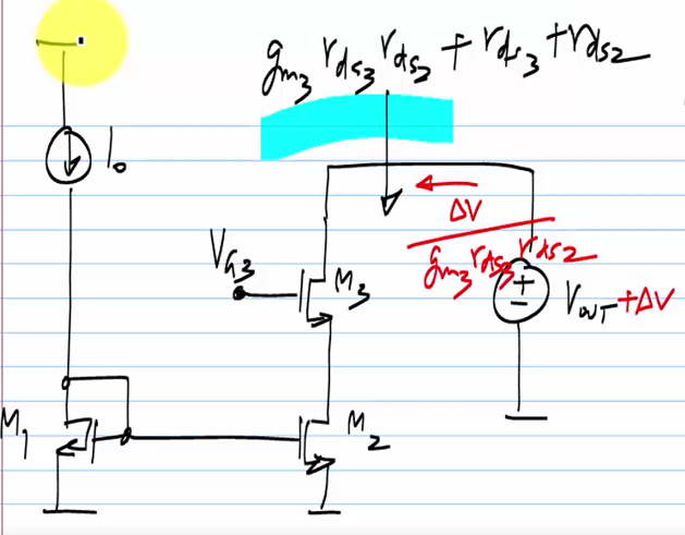
As a quick hand calculation of the new increased output resistance, it can be proven that the output resistance of a common source with degeneration is:


As a conclusion, since gm3*rds3*Rs >> Rs+rds3 a reasonable assumption is that output resistance in cascoded case is  gm3*rds3*rds2:
=> for a change of a delta Vout =>IDS1 changes to IDS1 + delta VDS1/(gm3*rds3*rds2) 
  • This is much less of IDS1 change comparing to the “non-cascode” original case


To get biasing VG3 = VGS1 + VGS3 we will add one more cascoded NMOS transistor M4 ( diode connected) at the branch of M1,   and the size of M4 should be the
same as the size of M3:


And now let’s get even more ambitious: here is now a calculation of a minimum voltage Vout so both ( simple and cascode ) current mirror to be operational  
  • cascode  minimum voltage is much higher than one in simple current mirror


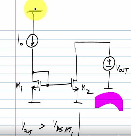
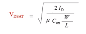
For a simple ( non cascoded ) current mirror Vout must be always greater than VDsat of M2 ( based on ID1=10uA ):


And for the cascoded case:


A minimum Vout for the current mirror to be operational:
Vout - VS4 > VG4 -VS4 -Vth
=> Vout  > VG4 -Vth
VG4 = VGS1 +VGS3
=> Vout  > VGS1 +VGS3  -Vth
=> Vout  > ( VGS1 -Vth) +( VGS3 -Vth )  +Vth
=> Vout > VDS1(saturation ) + VDS3(saturation ) + Vth
As a conclusion, by populating the Vout minimum expression with the simulation results and under assumption that Vth is approx. 760mV we are expecting for
the current topology/schematic  Vout minimum is :
Vout > 388mV + 406mV + 760mV = 1.556V
Since our alim. VDD=3.3V and so far for the current topology/schematic Vout min is approx. 1.556V the conclusion is: we don't have that much of a “headroom”. 
=> So, what we would really like is  a solution with a minimum possible value for the Vout min.
  • What is the minimum Vout for the current mirror to be operational  ?


A friendly reminder: A minimum Vout for the current mirror to be operational is driven by a minimal VG3 since:
Vout  > VG3 - Vth


What should it be a bias voltage of M4 (VG3 = ?), but it’s minimum value to remove any inefficiency ?
To achieve minimum VG3, a necessary condition is that M2 and M3 are in saturation ( VDS2 = VDS2(saturation)  and VDS3 = VDS3(saturation) )
=> VG3 = VGS3 ( when I0 current is flowing through M3,M2 ) + VDS2(saturation, again when I0 current is flowing through M3,M2  )
  • VG3 = VGS3 +VDS2 sat


Also in the case of the minimum VG3,  the minimum voltage Vout = VDS2( saturation, with I0 flowing through M2,M3) + VDS3(  saturation, with Io=10uA flowing through M2,M3).
=> according to our simulations so far we could expect for minimum VG3: 
Vout > 388mV + 406mV meaning: Vout min = approx. 800mv 


Our bias task related to M3, is to find what is ( and how to implement it ) VG3 = VGS3 ( when Io=10uA current is flowing through M2,M3 ) + VDS2(saturation, again when Io
current is flowing through M2,M3  ).
=> VG3 = VGS3 + VDS2(saturation)
VDS3(saturation) > VGS3 -Vth
since VGS3 -Vth = VG3 -VS3 -Vth and  VS3 = VDS2(saturation)
=> VGS3 -Vth = VG3 - VDS2(saturation) -Vth
=>   VDS3(saturation) > VG3 - VDS2(saturation) -Vth
=> VG3 > VDS3(saturation)  + VDS2(saturation) + Vth
=> VG3 minimum  = VDS3(saturation) + Vth +  VDS2(saturation)
Since:
Under assumption that sizes M3=M2 meaning both has the same W/L and Id3=Id2=10uA
=> VG3 minimum =  Vth + 2* VDS
=>VG3 = Vth + 2*2I0/(*Cox*W/L)
=>VG3 = Vth + 2I0/(*Cox*(W/4)/L)


What is 2I0/(*Cox*(W/4)/L) ? 
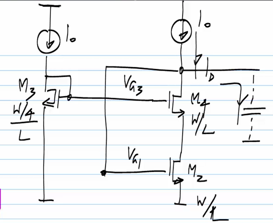
e.g. one way to look at this: 2I0/(*Cox*(W/4)/L) is a VDS( or Vov: “overdrive voltage”) of a transistor in saturation that has Id=I0 current, and has dimensions (W/4)/L .


In general, when faced with a need to generate a voltage Vth + something ( e.g.Vov ) we can use this structure, which is a transistor connected as a diode and always in guaranteed saturation:. 
  • VDS = VGS and  VDS saturation > VGS -Vth =>  always is true that VGS > VGS - Vth =>  the transistor is always in saturation )
=>
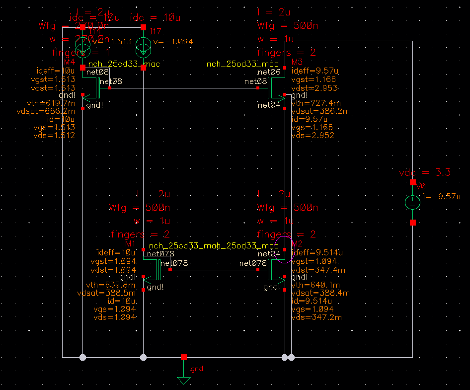
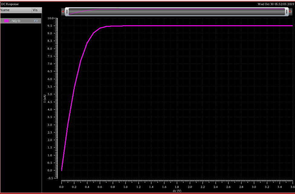
Also “sweeping” Vout=V0 shows that Vout minimum is around 0.8V in line with our hand calculation:


But there is a problem here: VDS1 (M1 transistor) and VDS2 (M2 transistor but minimum VDS2 to keep M2 in saturation  ) are not the same and Id3=Id2 of approx 9.57uA
will not be exactly Id1=10uA.
This is because of the influence of channel length modulation, in other words there will always a systematic error. So this schematic is good but it would be better if VDS1 = VDS2.
VDS2 is VDsat and VDS1 is VGS1 ( and  VGS1 = VDsat + Vth )  


So again the problem is how to implement a circuit to give us a perfect VGS1 to produce exactly VDS1 = VDS2 =>   Id3=Id2 equal exactly 10uA. 
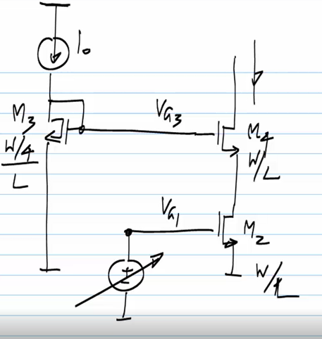
Let’s say we can find a perfect VGS1 ( to produce exactly VDS1 = VDS2 =>   Id3=Id2 equal exactly 10uA ) using a circuit like this:


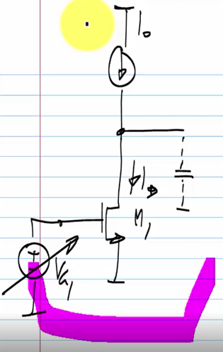
An equivalent circuit exists if we have a current source Io and transistor M1 how do we insure that Id1=10uA. We could take a voltage generator VG1 and adjust VGS1
to be exactly the value so  Id1=10uA:


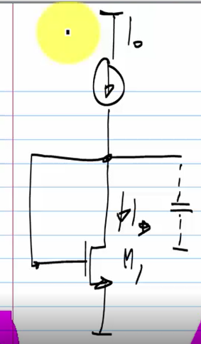
To get exact value of VG1=VGS1 to have ID1=Io=10uA we could use a circuit like this:


And finally let’s use the same principle in our original circuit:


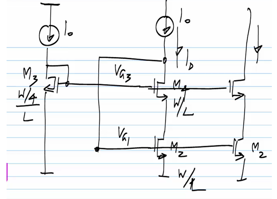
As a very final step we would just add one more current mirror branch:
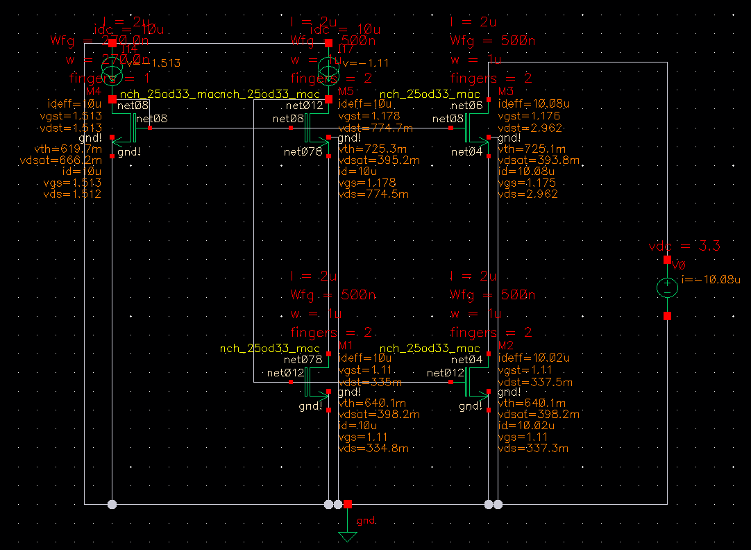
Here is the result of DC simulation of our TSMC 22nm circuit:
  • And this is called “High Swing Cascode” current mirror


Or a little bit different rearranged the same schematic:
Also we could use the same circuit with half a current value of the current referance(s): 5uA and burn less power :
 © 2011-2020 ASIC Stoic. All rights reserved.


Tuesday, October 29, 2019

Cadence Virtuoso CMOS Analog Design Basics in TSMC 22nm: “Constant gm bias circuit” with start-up and reduced sensitivity to changes in VDD

Cadence Virtuoso CMOS Analog Design Basics in  TSMC 22nm: “Constant gm bias circuit” with start-up  and reduced sensitivity to changes in VDD


In the previous blog post: “Cadence Virtuoso CMOS Analog Design Basics: a schematic for generating a reference current ( e.g. 10uA ) in a new techno ( e.g. TSMC 22nm )
using “Constant gm bias circuit”  with start-up” I didn’t pay attention to what is my circuit sensibility to changes in VDD .


A friendly reminder of the previous blog spot schematic:


A problem: the previous blog spot schematic sensibility to changes in VDD:


One solution to the problem of increased sensitivity of our “Constant gm bias circuit” to changes in VDD is very well described in James Baker book “CMOS 
Circuit Design, Layout, and Simulation” and his online available lectures.


The cause of the problem of the  large sensitivity to changes in VDD are low output resistance on NMOS transistors M4 and M5 because of “short channel”
technology TSMC 22nm. 
As a consequence of the low output resistance there increased sensibility of M4 and M5 current to changes in VDS4 and VDS5 caused by VDD changes.


As a conclusion  we need to reduce the variations in the drain-to-source 
voltages  of the NMOS  devices M4 and M5  with changes in VDD and to do this we will:
  • Disconnect gate drain connection of PMOS transistor M7
  • Add opamp   in negative feedback ( like it is almost always used ) that will  keep drain-to-source voltages ( of the NMOS devices M4 and M5 ) always the
  • same independent of VDD changes
    • The  idea is  to use the  amplifier to compare the drain voltage of M4 with the drain voltage of M5 and regulate them  to be equal:


Now the question is where to connect  “+” and where to connect “-” input of opamp ?


By the way It can be proven that Rout of M5 > Rout of M4 .


Here is how the negative feedback operates illustrated on an  example: 
  • when gate of M6/M7 goes down ( e.g. because of  because of a VDD change .. ), increasing currents ID6 = ID4 and ID7 = ID5 , 
  • => this will cause that VDS5 rise more than VDS4 and finally that this rise of VDS5 more than VDS4
  • => this will cause  that gate voltage of M6/M7 goes up ( and compensate that it went down in the first place ).
=> “+” input of op-amp should be connected to the drain of NMOS transistor M5.


Before I introduce op-amp to the schematic let’s go through an intermediate step and introduce Voltage Control Voltage Source ( vcvs ) from Cadence Virtuoso library
analogLib as a good approximation of  opamp especially if we setup in vcvs a Voltage Gain parameter ( A ) to some high value ( e.g. A = 10000 or 20*log 10000 = 80db )


Here we can see an improvement in much less sensitivity of Iref = 10uA on VDD changes.

Note*: Just a friendly reminder so far we did experiments assuming Voltage Gain = 10 000 ( 80 dB ) but in reality a single stage simple op amp that we are going to use
here will have more Voltage Gain = 50 ( 20*log (50) approx. 34dB.
  • To get to A > 100dB we would need to add a second “gain” stage ( additional  too.