Wednesday, October 16, 2019

Cadence Virtuoso CMOS Analog Design Basics: an example of adding a schematic for generating a reference current ( e.g. 10uA ) in a new techno ( e.g. TSMC 22nm )

Cadence Virtuoso CMOS Analog Design Basics: an example of adding a schematic for generating a reference current ( e.g. 10uA )  in a new techno ( e.g. TSMC 22nm ) 

Hi,


In this blog entry I will finish the previous design by adding schematic for generation 10uA current source. The topology chosen here is something called:
“Constant gm bias circuit” or “Beta-multiplier reference circuit”.

Note*: a MOSFET implementation of a Constant gm bias circuit is very well explained by prof. Jacob Baker in his book “CMOS Circuit Design, Layout, and  Simulation” or
in his university lectures available online. 
  • Here is a quick explanation of the basic idea of the MOSFET implementation of a Constant gm bias circuit 

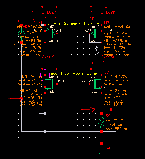
    • Let’s start with this schematic:


Note*: I covered some transistors sizing W and L information ( covered L’s and W’s that might not be
Wmin and Lmin any more in the final schematic ) in order to explain step by step how I got these
 transistor sizes. The same applies for the resistor value R0.
  
Now let’s say I am able to force ( somehow) the same Iref=10uA current through both transistors.
  • Obviously in this case width W of transistor M5 and width  W of transistor M4 are not the same so let’s assume : W(of transistor M5)= k*W(of transistor M4)

    • Note* For the moment I am choosing lengths L of both transistors to be the same


In order to force 10uA  current through M5 ( and M4 ) let’s add a pmos current mirror on the top, designed in such a way to give as the 10uA  current through M5 and M4.

  • A friendly reminder: as in previous blog entry these are  TSMC 22nm process RF NMOS and PMOS transistors that I have chosen to use for the schematic :


  • Please tell me if I am wrong but I concluded that need alim of VDD = 2.5V to use this techno/transistors.


Next I need to  size the four MOSFET transistors ( NMOS: M4, M5 and PMOS: M6, M7 ) and choose a value for resistor R to achieve my goal of having Iref = 10uA.
  • As a starting point I have chosen default minimum size:  Lmin, Wmin and NRmin( finger number) for all TSMC 22nm RF NMOS PMOS transistors

  • except M4 that we know has to have its W four times the W of the transistor M5:

In the next step I “sweeped” resistance R while observing ID5 t get ID5=10uA and  found that I need R=28K.
  • So here is a final schematic of “Constant gm bias circuit” producing the reference current of  Iref=10uA i

  • mplemented with minimum sizes of TSMC 22nm RF NMOS PMOStransistors and R=28K:

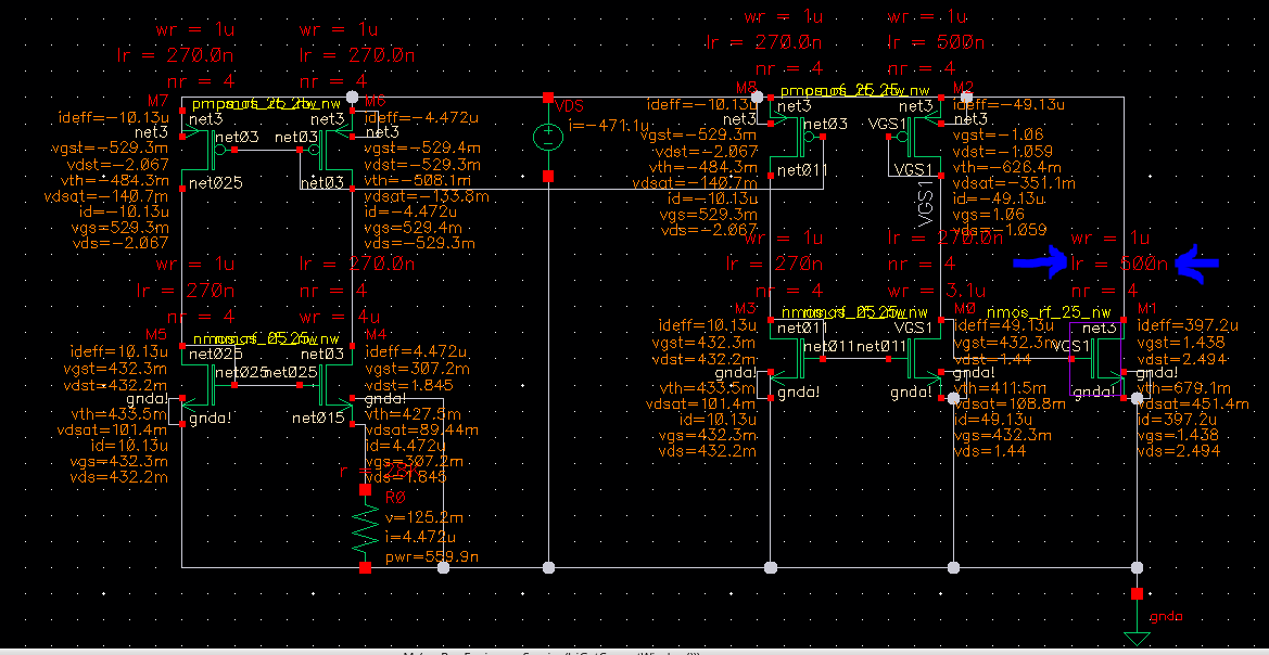
As a last step I will connect this Iref source circuit where I needed it in the schematic of the previous blog entry:


And here is a final schematic with the last adjustment in L of NMOS transistor M1 ( old L=350nm and the new one L=500nm )
to get as close as possible to its desired current of 400uA ( to be precise it is achieved ID1=397uA ).:


© 2011 ASIC Stoic. All rights reserved.

Tuesday, October 15, 2019

Cadence Virtuoso CMOS Analog Design Basics: an example of transistor sizing when using the first time new techno ( e.g. TSMC 22nm ) and we need NMOS transistor in saturation with ID=400uAV

Cadence Virtuoso CMOS Analog Design Basics: an example of transistor sizing when using the first time new techno ( e.g. TSMC 22nm ) and we need NMOS transistor in saturation with ID=400uAV

Hi,


I just got into new TSMC 22nm techno  and I wanted to bias one of its NMOS RF transistors using 10uA current source , to get ID=400uA.


This is an TSMC 22nm  RF NMOS and PMOS transistors that I have chosen to use for the task:


Please tell me if I am wrong but I concluded that need alim of VDD = 2.5V to use this techno/transistors.


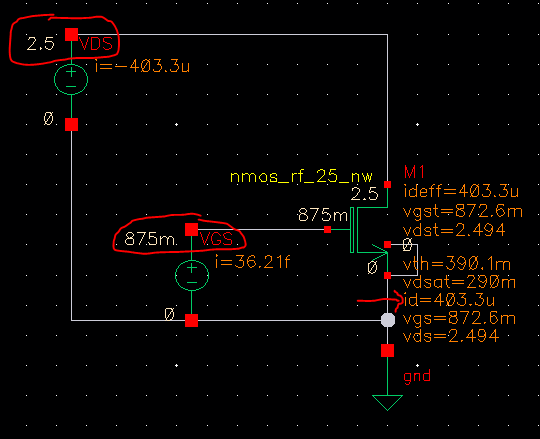
In a first step  setup a schematic ( like this one bellow)  and after VGS voltage DC sweep ( observing transistor ID current )
I got that, for VDD=2.5V as constant, for VGS=875mV I am getting desired Id approx. 400uA ( or to be exact .403.3uA ).


Note*: for TSMC 22nm  RF NMOS transistor I kept for the moment a default minimum size:  Lmin, Wmin and NRmin( finger number):


Next step is to bias M1 transistor with VGS1=875mV. 
Here is a topology used to get biasing of M1 transistor and as a friendly reminder I assume that I have on my disposal a current of 10uA and I want that M1  ID=400uA.


Note*: I covered some transistors sizing W and L information ( covered L’s and W’s are not Wmin and Lmin any more in the final schematic ! ) in order to explain step by step how I got these  transistor sizes.


 As a first step I did a quick experiment where I put all transistors on their default sizes but in DC simulation  I got M1 ID too high: 1.589mV related to my desired 400uA 
  • This is because VGS1 = VDS of  a transistor M0 is to high 1.82V related to desired  VGS1 = 0.872mV


Since this is the transistor equation used for the sizing calculation:


in the next step I tried to increase M0 transistor W in order reduce its VDS=VGS1 and consequently to reduce ID of transistor M1.


Unfortunately even if I used maximum M0 transistor W = 10uA ( still keeping Lmin and NRmin , finger numbers ) 
ID of transistor M1 was better than before but still too high: 1.16mA ( a friendly reminder: the desired value is 400uA )


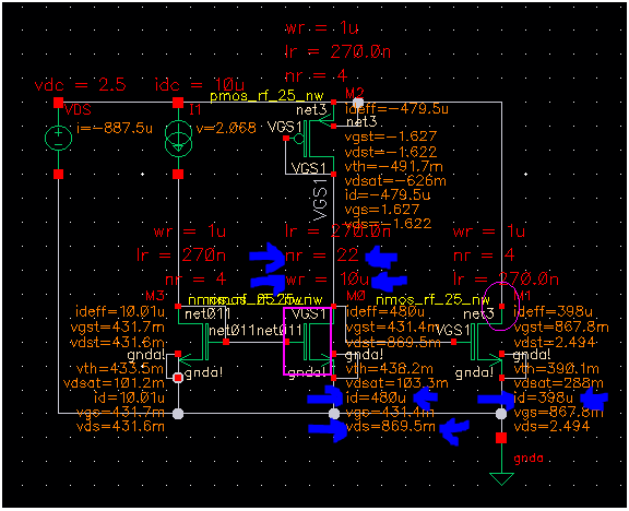
In the next step I kept maximum M0 transistor W = 10uA but I did a sweep NR( finger number maximum 32 ) and for NR=22 I got the desired current of M23 ID approx. 400uA:


But this “brute force” solution is using too big M0 transistor that is burning a lot of power:, transistor M0 ID0 = 480uA.


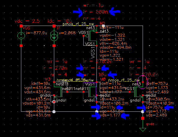
Let’s try another approach, I will keep transistor M0 Wmax=10uA ( still keeping Lmin and NRmin)  but I will increase L of PMOS transistor to Lmax=500nm.
  • This approach should  increase voltage VDS=VGS of transistor M2 and as result decrease VGS1 and transistor M1 ID current (  a new value of M1 ID current = 757uA while burning ID0 = 111uA of transistor M0 )


 In the last step, to reduce transistor M1 ID1 current from 757uA to desired 400uA, I did a parameter sweep of transistor M1 L ( while observing  M1 ID1 current ) and
for the value transistor M1 L=350nm => transistor M1 ID1 became approx. 400uA ( to be exact: transistor M1 ID1=407.9uA ):


© 2011 ASIC Stoic. All rights reserved.

Monday, October 14, 2019

Part #3: CMOS Analog Design Basics: an example of transistor sizing when using the first time new techno ( e.g. 1um ) and we need NMOS transistor in saturation with ID=400uA and VGS bias is 1.5V

Part #3: CMOS Analog Design Basics: an example of

transistor sizing  when using the first time new techno

( e.g. 1um ) and we need NMOS transistor in saturation

with ID=400uA and VGS bias is 1.5V


Hi, 


As a friendly reminder in the first document of the series: “CMOS Analog Design Basics: an example
of transistor sizing  when using the first time new techno ( e.g. 1um ) and we need NMOS transistor
in saturation with ID=400uA and VGS bias is 1.5V” as a title said our goal was to use these input data:
  •  1μ techo ( here is a Spice models of CMOS transistors ):
  • Alim. of Vdd =5V
  • Assuming bias VGS=1.5V


To achieve ID=400μA .


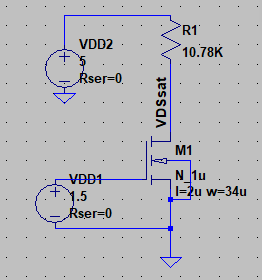
And in the past,  for this purpose I have chosen the following schematic:


 For the schematic I calculated and adjusted in simulation  the NMOS transistor sizing W/L=17 and
LTspice simulation showed: IDS = approx.  398 μA and VDSsat= approx. 711mV.


 And in the second document of the series: “PART#2: CMOS Analog Design Basics: an example of
transistor sizing  when using the first time new techno ( e.g. 1um ) and we need NMOS transistor in
saturation with ID=400uA and VGS bias is 1.5V” I replaced R1 with a diode connected PMOS
( and calculated it’s sizing W/L ):


Now I would like to bias transistor M1 with a necessary bias of VGS1=1.5V and for that
I am assuming that I have on my disposal  a current source of 20uA.


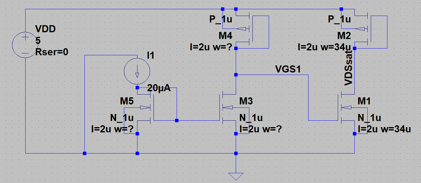
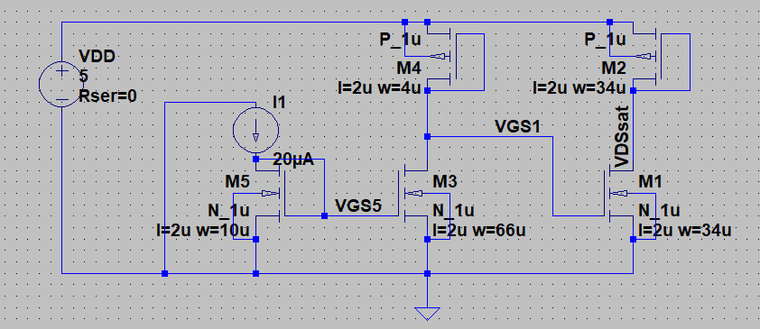
Here is a schematic ( “topology”) I am planning to use:


The basic idea of achieving transistor M1 biasing with VGS1=1.5V is to choose VSG4 of PMOS
transistor  M4 in such a way that VDD - VSG4 = 1.5V 


This is transistor equations ( a MOSFET transistor in saturation ) used for the sizing calculation:


Note*: As in previous schematics I decided to keep all MOSFET transistor length to one fixed
value: L=2um.


Also I need to take care that M3 stays in saturation when VGS1=1.5 V because VGS1= VDS3sat and
to do this I need to provide that VDS3sat > VGS3 -VTO(nmos). 
  • Since from Spice model of my NMOS transistor I know that


 => 1.5V > VGS3 - 0.8V
=>  2.3V > VGS3


Since VGS5=VGS3 , this means that I cannot choose sizing of NMOS transistor M5 to have
VGS3 > 2.3V so let me choose a convenient value VGS3=1.05 V.


Note* I have chosen VGS3=1.05 V because of my previous knowledge about this technology
mainly summarised from the following table:


To simplify our calculation let’s say that in our current mirror transistors M3 and M5 are equivalent in
size and also that we want to adjust our topology to have ID3=ID5=I1=20uA.


Also let’s temporary  simplify our topology replacing transistor M4 with a resistor R of unknown size
for the moment:


By doing simulation using parameter R1 “sweep” we will find value of R1 ( r1 approx. 174K ) to give
us VGS1=1.5V, keeping ID3=20uA.


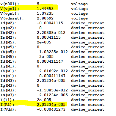
And really when for R1=174K we are getting biasing voltage VGS1=1.5V while keeping currents
equal: I1=ID3=ID5=IR1=20uA:


The last step is replacing resistor R1 with PMOS and calculation of the size of the PMOS was already
explained in previous blog post:  “Part #2: CMOS Analog Design Basics: an example of transistor
sizing when using the first time new techno ( e.g. 1um ) and we need NMOS transistor in saturation
with ID=400uA and VGS bias is 1.5V


But I made an assumption that I could achieve VGS1= 1.5V by having ID3 = ID4=10uA .
Let’s see if it is possible to size PMOS transistor M4 to do this.


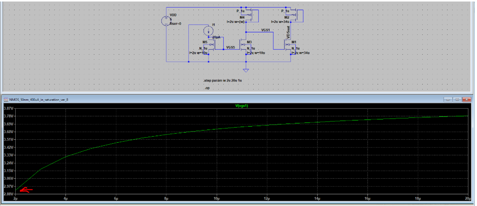
By doing simulation using parameter PMOS transistor M4 W “sweep” it is clear this is impossible:
even for a small value of W=2u VGS1 is more than 2.9V:


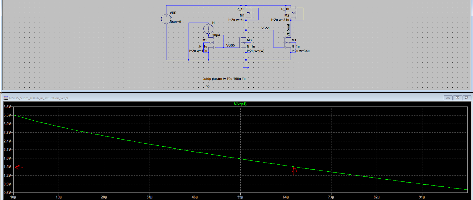
So I decided to choose a small value for PMOS transistor W=4u and then to “sweep”
NMOS transistor M3 W for a value large enough to increase current ID3=ID4 so VGS1
can fall to the desired value VGS1=1.5V:


Indeed for an NMOS transistor M3 with size  W=64 there is VGS1 approx.1.5V:


© 2011 ASIC Stoic. All rights reserved.

Friday, February 8, 2019

Part #2: CMOS Analog Design Basics: an example of transistor sizing when using the first time new techno ( e.g. 1um ) and we need NMOS transistor in saturation with ID=400uA and VGS bias is 1.5V


Hi,


As a friendly reminder in the first document of the series: “CMOS Analog Design Basics: an example
of transistor sizing  when using the first time new techno ( e.g. 1um ) and we need NMOS transistor
in saturation with ID=400uA and VGS bias is 1.5V” as a title said our goal was to using these input
data:
  • 1μ techo ( here is a Spice models of CMOS transistors ):
  • Alim. of Vdd =5V
  • Assuming bias VGS=1.5V


To achieve ID=400μA .


And in the past,  for this purpose I have chosen a following schematic:


For the schematic I calculated and adjusted in simulation  the NMOS transistor sizing W/L=17 and
LTspice simulation showed: IDS = approx.  398 μA and VDSsat= approx. 711mV.


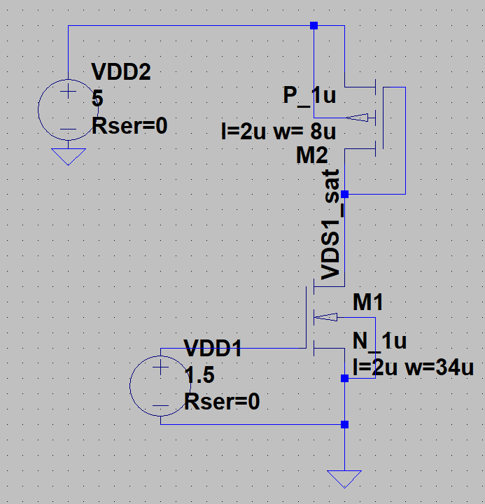
Now I would like to replace R1 with a diode connected PMOS ( and calculate it’s sizing W/L ):


To keep everything the same it should be:  ID2 = 400 μA and VDS1_sat= VD2 = 711mV.
=> VSD2 in saturation is equal: VSD2_sat = VDD - VDS1_sat
=> VSD2_sat should be  equal: VSD2_sat = 5V - 711mv = 4,289 V

This is the transistor equation used for the sizing calculation:


  • μ  of PMOS is from the Spice model :


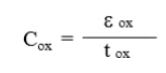
  • Step 1: Cox is calculated using following formula:


where is a constant:
and ( units are meters[m] ) is from Spice model of the transistor:


  • Here is a spreadsheet to calculate Cox:


P-mos ( techno data )


P-mos ( calculated data )

TOX[m]
UO [cm^^2/Vsec]

Cox[F/meter ^^2)
Cox[fF/micro meter ^^2)
2.00E-08
250

1.73E-03
1.73E+04


Or here is an Octave program that do the same Cox calculation:
#include <octave/oct.h>
syms ID min eox tox WdivL VGS VTH Cox min_times_Cox VDSsat R VDD
 
e0x = 3.9*8.854*power(10, -12) ;
 tox = 200*power(10,-10)        ; % units: m
 min = 250                      ;
 VDD = 5                        ;
 
 Cox = e0x/tox                  ;
 
 disp( "Cox =" ),  disp( Cox ), disp( "units: F/m2" ) ;
 
 Cox = (e0x/tox)*( power(10,15)/power(10,8) ) ;                
 
 disp( "or Cox =" ),  disp( Cox ), disp( "units: fF/micro-m2" ) ;

Result of the Octave  program run:
Cox =
0.0017265
units: F/m2
or Cox =
  1.7265e+04
units: fF/micro-m2


  • Step 2:  Calculating  Cox * μ pmos (units: F/Vsec)


    • Here is a spreadsheet to calculate Cox * μ :


P-mos ( techno data )


P-mos ( calculated data )


TOX[m]
UO [cm^^2/Vsec]

Cox[F/meter ^^2)
Cox[fF/micro meter ^^2)
Cox[F/micro meter ^^2)*UO [cm^^2/Vsec]=
Cox[F/micro meter ^^2)*UO [micro meter ^^2/Vsec]*10^^4[fF/micro meter ^^2]=
Cox[F/micro meter ^^2)*UO [micro meter ^^2/Vsec]*10^^4*10^^-15[F/micro meter ^^2]
2.00E-08
250

1.73E-03
1.73E+04
4.31632500E-05


Or here is an Octave program that do the same Cox * μ calculation:

#include <octave/oct.h>
 syms ID min eox tox WdivL VGS VTH Cox min_times_Cox VDSsat R VDD
 
 e0x = 3.9*8.854*power(10, -12) ;
 tox = 200*power(10,-10)        ; % units: m
 min = 250                      ;
 VDD = 5                        ;
 
 Cox = e0x/tox                  ;
 
 disp( "Cox =" ),  disp( Cox ), disp( "units: F/m2" ) ;
 
 Cox = (e0x/tox)*( power(10,15)/power(10,8) ) ;                
 
 disp( "or Cox =" ),  disp( Cox ), disp( "units: fF/micro-m2" ) ;
 
 min_times_Cox = min * Cox * power(10,4) * power(10,-15) ;
 disp ( "min * Cox =" ), disp( min_times_Cox ), disp( "units: F/Vsec" ) ;


Result of the Octave  program run:
Cox =
0.0017265
units: F/m2
or Cox =
  1.7265e+04
units: fF/micro-m2
min * Cox =
  4.3163e-05
units: F/Vsec


  • Step 3:  Calculating  W/L

    • Summary:
      • Reminder, this is the equation we are using:
      • We know that we want:
        • ID1 = ID2 = 400μA


      •  We know we need M2 transistor in saturation :
        • VSD2_sat = 5V - 711mv = 4,289 V


      • From techno, meaning from SPICE model,  the value of Vth[V] of a PMOS transistor  is:


  • We already calculated  Cox * μ [F/Vsec] = 1.7265*10^^4


=> W/L of M2 PMOS = 1.637 or approx. 2

Here is an Octave program that do the same W/L calculation:


#include <octave/oct.h>
 syms ID min eox tox WdivL VGS VTH Cox min_times_Cox VDSsat R VDD
 
 e0x = 3.9*8.854*power(10, -12) ;
 tox = 200*power(10,-10)        ; % units: m
 min = 250                      ;
 VDD = 5                        ;
 
 Cox = e0x/tox                  ;
 
 disp( "Cox =" ),  disp( Cox ), disp( "units: F/m2" ) ;
 
 Cox = (e0x/tox)*( power(10,15)/power(10,8) ) ;                
 
 disp( "or Cox =" ),  disp( Cox ), disp( "units: fF/micro-m2" ) ;
 
 min_times_Cox = min * Cox * power(10,4) * power(10,-15) ;
 disp ( "min * Cox =" ), disp( min_times_Cox ), disp( "units: F/Vsec" ) ;

f = -ID + (1/2)*min_times_Cox*(WdivL)*power((VGS-VTH),2)

% Substitute in values that are known
 newf = subs(f, [ID VGS VTH], [( 400*power(10, -6) ), (VDD - 0.711), 0.9]);

% Solve the resulting symbolic expression for x
 result = solve(newf == 0, WdivL)


% And if you need a numeric (rather than symbolic) result
double(result)


Result of the Octave  program run:
Cox =
0.0017265
units: F/m2
or Cox =
  1.7265e+04
units: fF/micro-m2
min * Cox =
  4.3163e-05
units: F/Vsec
f = (sym)
   
result = (sym)

               
ans =  1.6137


As a sanity check let’s verify do we really have VSD2_sat = 5V - 711mv = 4,289 V when using M2 PMOS sizing W/L = 2 and after calculations result is VSD2_sat = 3.0442V ( expecting 4.289V )


Here is an Octave program that do the same VSD2_sat calculation:
#include <octave/oct.h>
 syms ID min eox tox WdivL VGS VTH Cox min_times_Cox VDSsat R VDD
 
 e0x = 3.9*8.854*power(10, -12) ;
 tox = 200*power(10,-10)        ; % units: m
 min = 250                      ;
 VDD = 5                        ;
 
 Cox = e0x/tox                  ;
 
 disp( "Cox =" ),  disp( Cox ), disp( "units: F/m2" ) ;
 
 Cox = (e0x/tox)*( power(10,15)/power(10,8) ) ;                
 
 disp( "or Cox =" ),  disp( Cox ), disp( "units: fF/micro-m2" ) ;
 
 min_times_Cox = min * Cox * power(10,4) * power(10,-15) ;
 disp ( "min * Cox =" ), disp( min_times_Cox ), disp( "units: F/Vsec" ) ;

f = -ID + (1/2)*min_times_Cox*(WdivL)*power((VGS-VTH),2)

% Substitute in values that are known
 newf = subs(f, [ID VGS VTH], [( 400*power(10, -6) ), (VDD - 0.711), 0.9]);

% Solve the resulting symbolic expression for x
 result = solve(newf == 0, WdivL)


% And if you need a numeric (rather than symbolic) result
double(result)


%%%%%%%%%%%%%%%%%%%%%%%%%%%%%%%%%%%%%%%%%%%%%%%%%%%%%%%%%%%%%
f = -ID + (1/2)*min_times_Cox*(WdivL)*power(VDSsat,2)


% Substitute in values that are known
 newf = subs(f, [ID WdivL] , [( 400*power(10, -6) ), 2 ]);
 
 % Solve the resulting symbolic expression for x
 result = solve(newf == 0,VDSsat)
 
 % And if you need a numeric (rather than symbolic) result
double(result)
Result of the Octave  program run:
Cox =
0.0017265
units: F/m2
or Cox =
  1.7265e+04
units: fF/micro-m2
min * Cox =
  4.3163e-05
units: F/Vsec
f = (sym)

result = (sym)

              ans = 1.6137
f = (sym)

       result = (sym 2×1 matrix)

 ⎡-√45409 ⎤
 ⎢────────⎥
 ⎢  70 ⎥
 ⎢       ⎥
 ⎢ √45409 ⎥
 ⎢ ────── ⎥
 ⎣  70 ⎦

ans =

 -3.0442
  3.0442

Source code of Octave program is here: octave program

  • Step 4:  Verifying that when we have an PMOS ( in the techno used ) with  W/L = 2 and and we want VSD2_sat = 4,289 V and alim. for this techno is VDD=5V, then the transistor M2 PMOS  should be in saturation with ID = 400μA


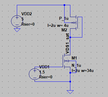
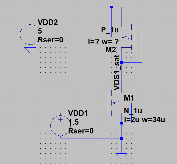
    • For this verification I will use LTSpice simulation of following schematic:

Note*: We expect VDS1_sat minimum to be VGS1 - Vth nmos = 1.5 - 0.8 = 0.7V


=> we expect that in this schematic  VDS2_sat max. = VDD - VDS1_sat min. = 4.3V


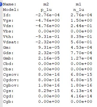
LTspice simulation showed: ID2=ID1 =  approx. 276 μA (expected 400 μA ) and VDS1_sat= 0.244V ( expected result: 711mV ) which is too low so  M1 is not even in saturation.


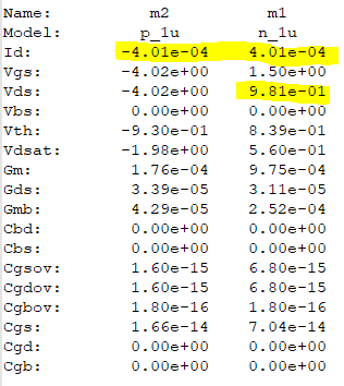
Finally, by adjusting  of M2 PMOS sizing W/L from 2 to 8,  LTspice simulation showed: ID1 = 400.1 μA   and VDS1_sat= 981mV


© 2011 ASIC Stoic. All rights reserved.