Friday, December 6, 2019

Cadence Virtuoso CMOS Analog Design Basics in TSMC 22nm: a simple op-amp design with a High Swing Cascode current mirror- Part 2

Introduction


In this blog post we will finally design a simple opamp that will reuse our High Swing Cascode current mirror.


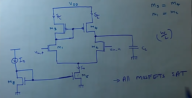
A design of a simple opamp is very well explained by  Hafeez KT, in his youtube lecture available online and here is a basic topology:
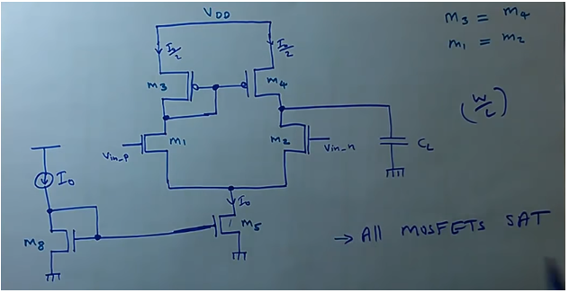
A summary of specification points that will be achieved in this opamp design:

  • our op amp has to drive capacitive load of C1 = 10pf with a 
  • Slew Ratio ( SR ) = 2V/second
  • Input Common Mode Range ( negative, minimum ):  ICMR- = 1.2V
    • Voltage on differential pair inputs should never be less than  1.2V
  • Input Common Mode Range ( positive, maximum  ): ICMR+ = 3.0V 
    • Voltage on differential pair inputs should never  not exceed 3.0V
  • Gain Bandwidth product ( GB ) > 3MHz)


Note* : L=1u for all transistors.


Calculation the value of current to be provided by M5 

A friendly reminder that our op amp has to have:
  • drive capacitive load of C1 = 10pf with a 
  • Slew Ratio ( SR ) = 2V/second
=>SR is rate of changing voltage across load capacitance C1
Q = C1 * V
dQ/dt = C1*dV/dt
I capacitance = C1*dV/dt
C1 is charging when differential pair branch M1/M3 is conducting ( consequently branch M4/M2 is not conducting ) with all the current I.
C1 is discharging when differential pair branch M4/M2 is conducting ( consequently branch M1/M3 is not conducting ) with all the current I.
Conclusion I of capacitance = I is:
=> I = C1*dV/dt
=> I = C1*SR
=> I = 10pF*2V/ u second = 20uA
=> I0 or ID5 = 20uA


Estimating ( by simulation )  p*Cox and n*Cox

for TSMC 22nm process PMOS and NMOS

transistor used

The technology that we are using here ( TSMC 22nm ) is new to me and I am
using pmos transistor pch_25od33_mac ( for M3/M4, pmos active load )  and I
don’t know its    


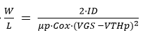
In general to calculate  W/L for M3/M4 we will use formula:
Then I setup a following simulation to find ( approx.) :
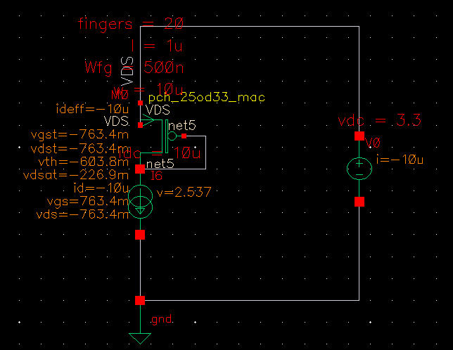
  • VDS = 3.3V
  • Idc = 10uA
  • W=10um
  •  L=1u
The DC simulation showed Vthp=603.8mV and Vgs=Vds=763.4mV
=> = 2*10uA/( ( 10um/1um) * (763.4mV - 603.8mV)^^2 ) 
=> = 7.85*( 10 ^^ -5 )
       Vth_p    = 603.8mV
Also I am using nmos transistor nch_25od33_mac ( for M1/M2, nmos differential pair  ) and here also I don’t know its n*Cox
Then I setup following simulation to find ( approx.) n*Cox
  • Idc = 10uA
  • W=10um
  •  L=1u
The DC simulation showed Vthn=672.2mV and Vgs=Vds=727.7mV
=> n*Cox= 2*10uA/( ( 10um/1um) * (727.7mV - 672.2mV)^^2 ) 
=> n*Cox= 649.2*( 10 ^^ -6 )
     Vth_n = 672mV 


Calculation of  W/L for M3/M4 ( pmos active load ) 

A friendly reminder of a points in specification:
  • Input Common Mode Range ( positive, maximum  ) , ICMR+ = 3.0V
    • Voltage on differential pair inputs should never  not exceed 3.0V


For calculation of  W/L for M3/M4 ( pmos active load ) let’s focus on highlighted transistors M1/M2:
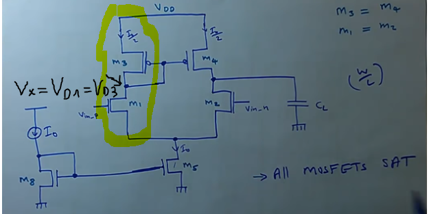


for transistor M0 to be in saturation VDS3 > VGS3 -Vth_p and ID1=ID3 = 10uA
if Vx = VD1 = VD3 and VDS1 > VGS1 - Vth_n => VD1 > VG1 - Vth_n
=> Vx > Vin_p -Vth_n
A friendly reminder: Vth_p    = 603.8mV and Vth_n = 672mV 


Maximum voltage on Vin_p = 3.0 V ( this is based on  ICMR+ = 3.0V ) and for Vin_p = 3.30V Vth-n=0.672

=>  Vx > 3.0V - 0.672 V = 2.328 V so we can adopt Vx  = VD1= VD0= 2.5V 
Since M0 is in saturation too, and VS0 = VDD :
=> VSD3 = VS3 -VD3 = VDD - 2.5 =3.3V -2.5  = 0.8V 
=> VDS0 =VGS0 = 0.8V 
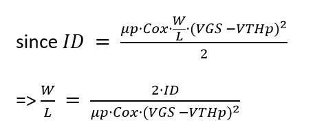
A friendly reminder: = 7.85*( 10 ^^ -5 )
=> W/L( PMOS M3) = 2*10uA/(79u*(0.8 -  0.604 )^^2 ) 


W/L( PMOS M3) =6.58 approx. 7


Calculation of  W/L for M1/M2 ( nmos diff. pair ) 


For calculation of  W/L for M1/M2 ( nmos differential pair ) let’s focus on highlighted transistors M4/M2:
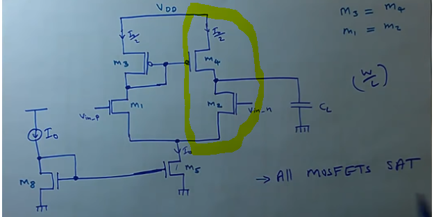

A friendly reminder of a couple specification points of our opamp::  
  • Gain Bandwidth product ( GB ) > 3MHz
  •  opamp is driving a capacitive load of 10pF


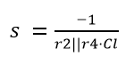
We will use formula GB=  DC gain * (first) pole
It can be proven that: 
  • First pole:
=>


gm2= 3MHz*2*3.14*10pF= 188u
And because M2= M1 => gm2 = gm1

Finally to calculate M1,2 W/L we will use a formula gm=f(ID, W/L):


A friendly reminder:
  •  Vth_p    = 603.8mV and Vth_n = 672mV 
  • = 7.85*( 10 ^^ -5 )
  • n*Cox= 649.2*( 10 ^^ -6 )


=>  W/L ( for NMOS M1 and M2 ) = 2.74 approx. 3  


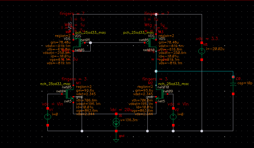
Fully transistor sized schematic ( but no current source implemented  yet )


Finally our ( fully sized transistors )  schematic ( after DC simulation with annotated DC operating points ) including:
  • Vdd = 3.3V
  • Vin = 1V

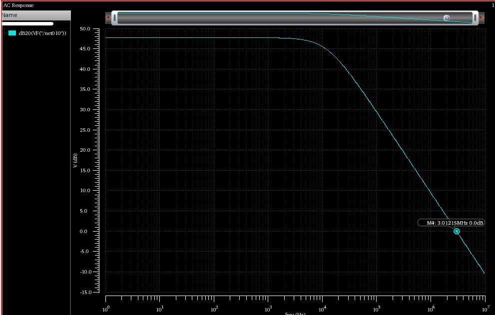
But did we achieve a point of the spec Gain Bandwidth product ( GB ) > 3MHz ?


A friendly reminder that Gain Bandwidth product is a frequency where 20log(output voltage/input voltage)=0dB and in our case Gain Bandwidth product is only 1.48MHz:
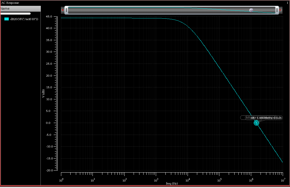


The lower than expected GB  is because a low value for gm of transistors
M1/M2 ( nmos differential pair ): gm1/2= 93.6u and to achieve
GB > 3MHz we calculated that gm1,2 should be gm1/2= 188u.
And to increase gm1,2 we need to further increase W1,2 to  W1,2=24u
to achieve gm1,2=188u :


Another useful check is to, in DC simulation,  “sweep” Vin from 0V to
3.3V ( VDD ) and to check that for  the range of valid Vin voltages (
ICMR- = 1.2V, ICMR+ = 3.0V )  all four transistors are in saturation:


Fully transistor sized schematic

Now we are replacing the ideal current source with High Swing Cascode
current mirror ( designed in the previous blog entry ):
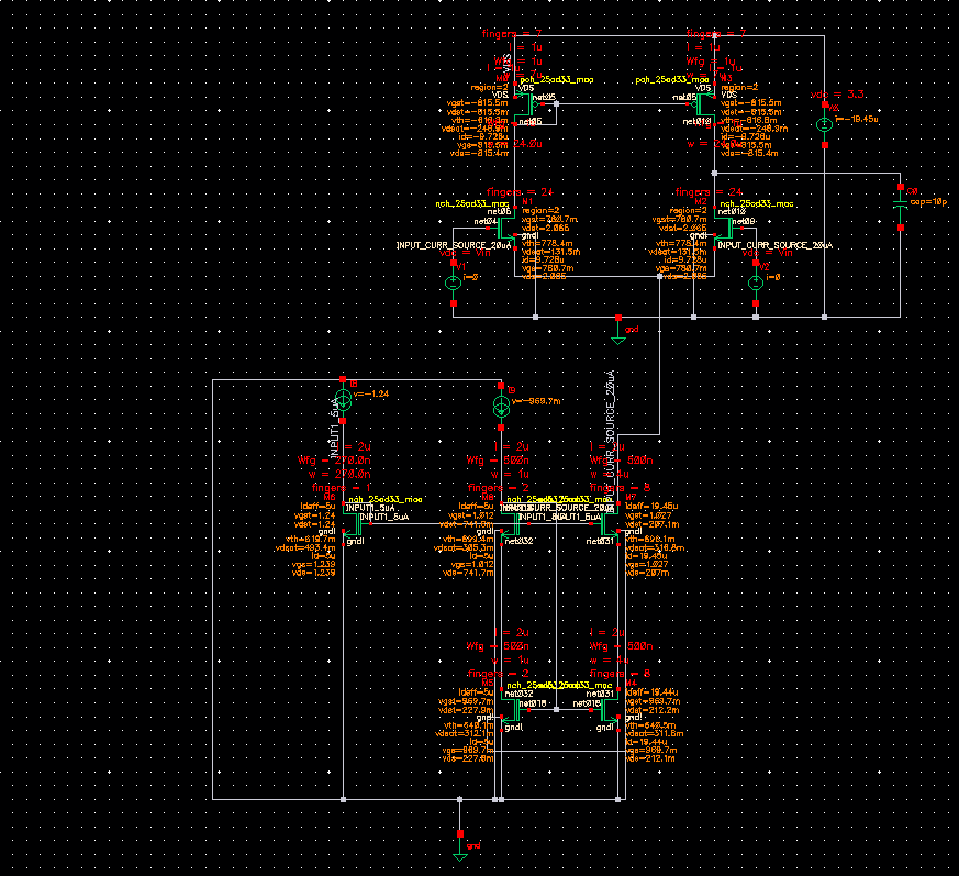

Again the  useful check to “sweep” Vin from 0V to 3.3V ( VDD ) in DC
simulation, and to verify  that for the range of valid Vin voltages ( ICMR-
= 1.2V, ICMR+ = 3.0V ) all four transistors of opamp core are in
saturation:
© 2019 ASIC Stoic. All rights reserved

Wednesday, October 30, 2019

Cadence Virtuoso CMOS Analog Design Basics in TSMC 22nm: a simple op-amp design with a High Swing Cascode current mirror

Cadence Virtuoso CMOS Analog Design Basics in  TSMC 22nm: a simple op-amp design with a High Swing Cascode current mirror


In the previous blog post “Cadence Virtuoso CMOS Analog Design Basics in  TSMC 22nm: “Constant gm bias circuit” with start-up and reduced sensitivity 
to changes in VDD” we needed to add an opamp.


A design of a simple opamp is very well explained by  Hafeez KT, in his youtube lecture available online and here is a basic topology:


But even the simplest opamp schematic would need a current mirror  ( NMOS transistors M5 and M8 ) provide necessary referent current Io .


In this blog post I  would like to explore  a High Swing Cascode current mirror a subject very well explained by prof. Nagendra Krishnapura  in his lectures
available online ( ee5320 2016 IIT Madras ).


For a “short channel” processes ( or other name is  a nanometer process ) such as TSMC 22nm , we should always use High Swing Cascode because 
ID5 is very dependant on VDS5 .


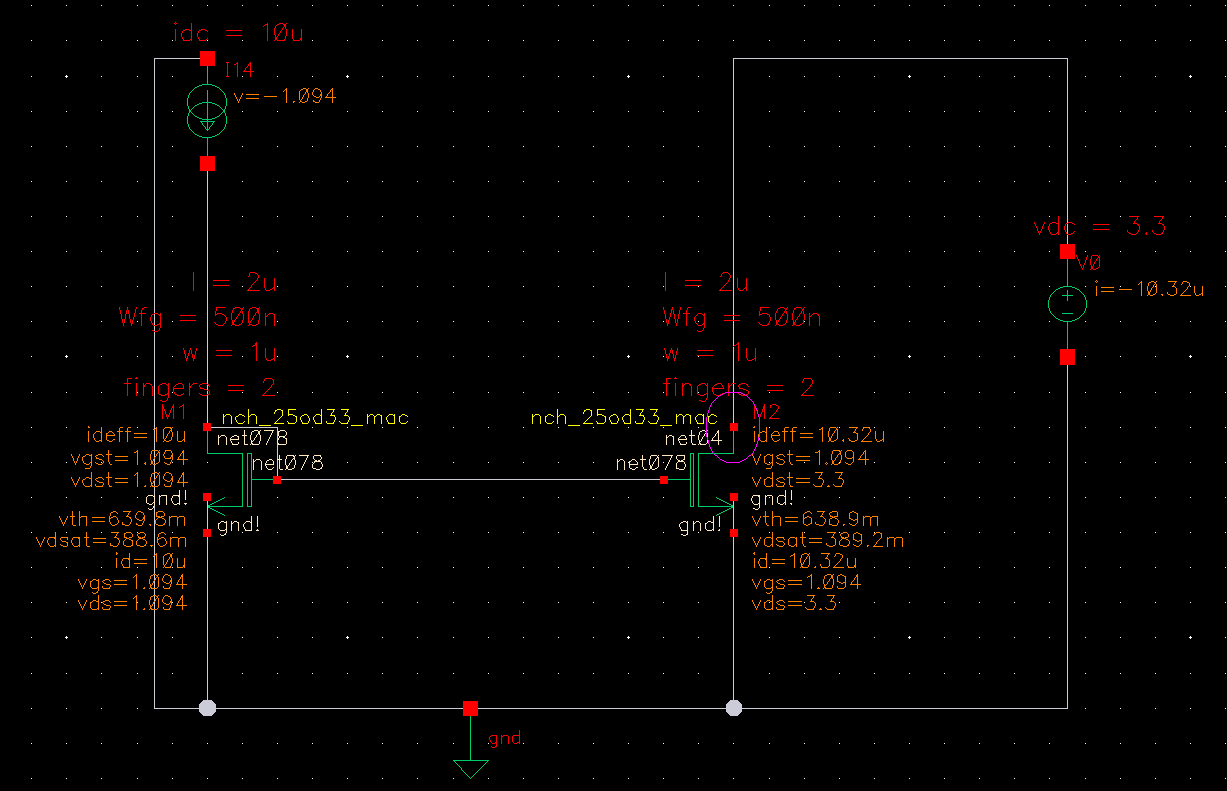
E.g. For VDS1=VDD = 3.3 ,  a change between VGS1=VGS2=1.094V to 3.6V is causing change of ID1 between: 10uA to 10.55uA. Expected value
ID2=ID1 = 10uA is true only if VDS1=VDS2=VGS1=VGS2=1.094V.


Variation of ID1 with a variation of VDD=VDS1 is no surprise because it can be proven that output resistance of M1 ( the resistance “seen” to the drain of M2 transistor) is 1/gds2 .
=> for a change of a delta Vout=VDS1 =>IDS1 changes to IDS1 + delta VDS1*gds2


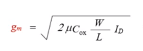
Since for NMOS transistor M2 in saturation gm is:


=> there are two solutions to the problem of the small output resistance: 
  • somehow  increase the output resistance  or 
  • decrease gm ( or decrease W, or increase L or increase ID2=ID1=Io=10uA )


Decreasing gm is not really an option because our referent current is 10uA and we don’t want to “burn” more current/power. On the other hand  W/L of transistors M1 and M2 is
W/L=1u/2u, a reasonable small W and a reasonable big value of L.


=> The solution is an increase of output resistance.


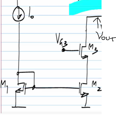
One of the solutions is to use a current buffer ( NMOS transistor M3 ). Current buffer would be a device that gives you the same current but a much higher output resistance.
  • A common gate stage is a current buffer ( cascoded transistor )


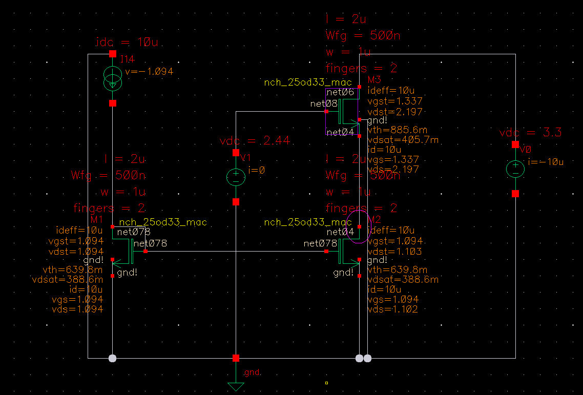
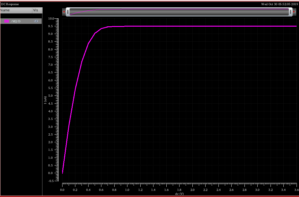
Biasing of NMOS transistor M3 could be found by “sweep” of V1= VG3 and at the same time observing ID1 to reach ID2=ID1=10uA.
  • The “sweep” value  of V1=VG3 to reach ID2=ID1=10uA is V1=VG3=2.441V which is in line with a following hand calculation:
    • Ideally M2 drain voltage should be VGS1 ( so M1 and M2 could be exactly the same and Id1 = Id2 = I0 ) and in reality  M2 drain voltage is
    • VG3 - VGS3 => ideally VGS1 = VG3 - VGS3 
    • => VG3 = VGS1 + VGS3
From simulation: VG3 =  VGS1(1.094V) + VGS3(1.337V) = 2.441V


Finally we achieved a much better stability of  IDS1 in relation to variation of VDD:
  • For a V0=Vout change from 1.18V to 3.6V, IDS1 change is from 9.99uA to 10uA:
    • Using cascoded transistor M3, we increased output resistance hence better result of the stable ID2=ID3=10uA with a variation of V0=Vout
Note*: The simulation shows that for this topology schematic developed so far,  V0=Vout minimum is around 1.18V which is high when we consider that alim. voltage
VDD=3.3V
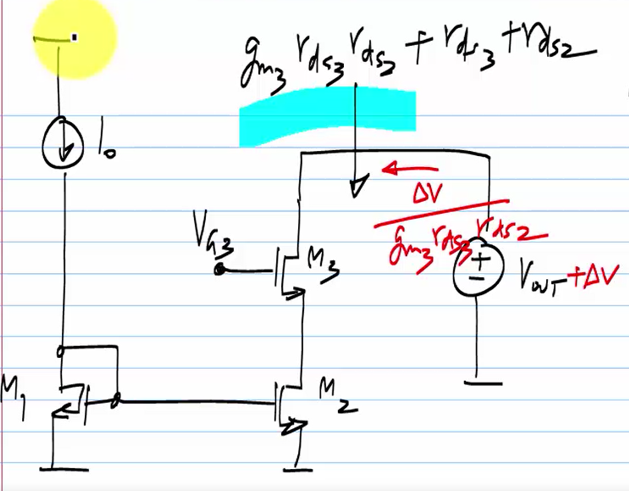
As a quick hand calculation of the new increased output resistance, it can be proven that the output resistance of a common source with degeneration is:


As a conclusion, since gm3*rds3*Rs >> Rs+rds3 a reasonable assumption is that output resistance in cascoded case is  gm3*rds3*rds2:
=> for a change of a delta Vout =>IDS1 changes to IDS1 + delta VDS1/(gm3*rds3*rds2) 
  • This is much less of IDS1 change comparing to the “non-cascode” original case


To get biasing VG3 = VGS1 + VGS3 we will add one more cascoded NMOS transistor M4 ( diode connected) at the branch of M1,   and the size of M4 should be the
same as the size of M3:


And now let’s get even more ambitious: here is now a calculation of a minimum voltage Vout so both ( simple and cascode ) current mirror to be operational  
  • cascode  minimum voltage is much higher than one in simple current mirror


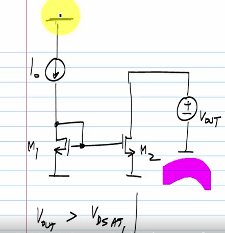
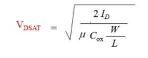
For a simple ( non cascoded ) current mirror Vout must be always greater than VDsat of M2 ( based on ID1=10uA ):


And for the cascoded case:


A minimum Vout for the current mirror to be operational:
Vout - VS4 > VG4 -VS4 -Vth
=> Vout  > VG4 -Vth
VG4 = VGS1 +VGS3
=> Vout  > VGS1 +VGS3  -Vth
=> Vout  > ( VGS1 -Vth) +( VGS3 -Vth )  +Vth
=> Vout > VDS1(saturation ) + VDS3(saturation ) + Vth
As a conclusion, by populating the Vout minimum expression with the simulation results and under assumption that Vth is approx. 760mV we are expecting for
the current topology/schematic  Vout minimum is :
Vout > 388mV + 406mV + 760mV = 1.556V
Since our alim. VDD=3.3V and so far for the current topology/schematic Vout min is approx. 1.556V the conclusion is: we don't have that much of a “headroom”. 
=> So, what we would really like is  a solution with a minimum possible value for the Vout min.
  • What is the minimum Vout for the current mirror to be operational  ?


A friendly reminder: A minimum Vout for the current mirror to be operational is driven by a minimal VG3 since:
Vout  > VG3 - Vth


What should it be a bias voltage of M4 (VG3 = ?), but it’s minimum value to remove any inefficiency ?
To achieve minimum VG3, a necessary condition is that M2 and M3 are in saturation ( VDS2 = VDS2(saturation)  and VDS3 = VDS3(saturation) )
=> VG3 = VGS3 ( when I0 current is flowing through M3,M2 ) + VDS2(saturation, again when I0 current is flowing through M3,M2  )
  • VG3 = VGS3 +VDS2 sat


Also in the case of the minimum VG3,  the minimum voltage Vout = VDS2( saturation, with I0 flowing through M2,M3) + VDS3(  saturation, with Io=10uA flowing through M2,M3).
=> according to our simulations so far we could expect for minimum VG3: 
Vout > 388mV + 406mV meaning: Vout min = approx. 800mv 


Our bias task related to M3, is to find what is ( and how to implement it ) VG3 = VGS3 ( when Io=10uA current is flowing through M2,M3 ) + VDS2(saturation, again when Io
current is flowing through M2,M3  ).
=> VG3 = VGS3 + VDS2(saturation)
VDS3(saturation) > VGS3 -Vth
since VGS3 -Vth = VG3 -VS3 -Vth and  VS3 = VDS2(saturation)
=> VGS3 -Vth = VG3 - VDS2(saturation) -Vth
=>   VDS3(saturation) > VG3 - VDS2(saturation) -Vth
=> VG3 > VDS3(saturation)  + VDS2(saturation) + Vth
=> VG3 minimum  = VDS3(saturation) + Vth +  VDS2(saturation)
Since:
Under assumption that sizes M3=M2 meaning both has the same W/L and Id3=Id2=10uA
=> VG3 minimum =  Vth + 2* VDS
=>VG3 = Vth + 2*2I0/(*Cox*W/L)
=>VG3 = Vth + 2I0/(*Cox*(W/4)/L)


What is 2I0/(*Cox*(W/4)/L)
e.g. one way to look at this: 2I0/(*Cox*(W/4)/L) is a VDS( or Vov: “overdrive voltage”) of a transistor in saturation that has Id=I0 current, and has dimensions (W/4)/L .


In general, when faced with a need to generate a voltage Vth + something ( e.g.Vov ) we can use this structure, which is a transistor connected as a diode and always in guaranteed saturation:. 
  • VDS = VGS and  VDS saturation > VGS -Vth =>  always is true that VGS > VGS - Vth =>  the transistor is always in saturation )
=>
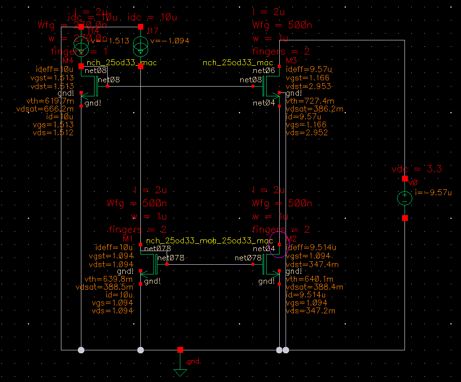
Also “sweeping” Vout=V0 shows that Vout minimum is around 0.8V in line with our hand calculation:


But there is a problem here: VDS1 (M1 transistor) and VDS2 (M2 transistor but minimum VDS2 to keep M2 in saturation  ) are not the same and Id3=Id2 of approx 9.57uA
will not be exactly Id1=10uA.
This is because of the influence of channel length modulation, in other words there will always a systematic error. So this schematic is good but it would be better if VDS1 = VDS2.
VDS2 is VDsat and VDS1 is VGS1 ( and  VGS1 = VDsat + Vth )  


So again the problem is how to implement a circuit to give us a perfect VGS1 to produce exactly VDS1 = VDS2 =>   Id3=Id2 equal exactly 10uA. 
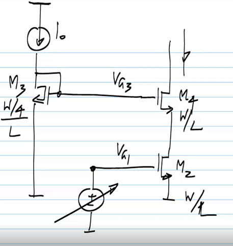
Let’s say we can find a perfect VGS1 ( to produce exactly VDS1 = VDS2 =>   Id3=Id2 equal exactly 10uA ) using a circuit like this:


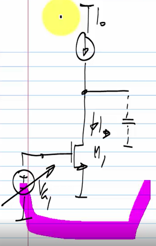
An equivalent circuit exists if we have a current source Io and transistor M1 how do we insure that Id1=10uA. We could take a voltage generator VG1 and adjust VGS1
to be exactly the value so  Id1=10uA:


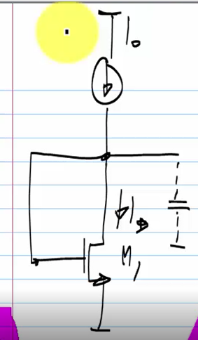
To get exact value of VG1=VGS1 to have ID1=Io=10uA we could use a circuit like this:


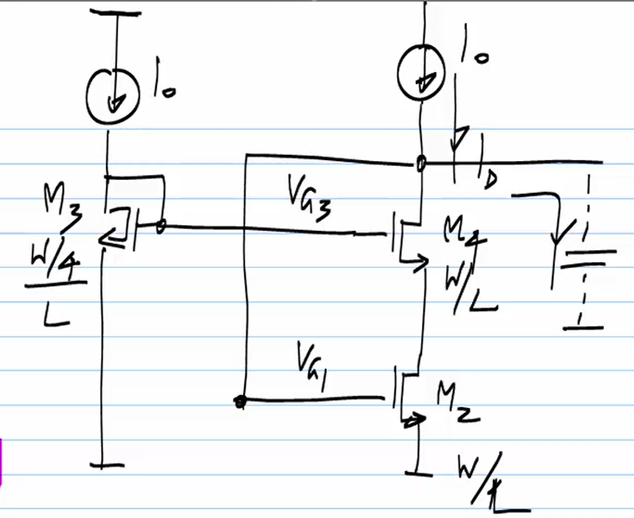
And finally let’s use the same principle in our original circuit:


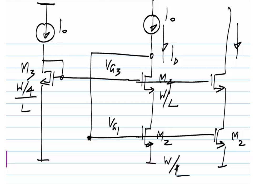
As a very final step we would just add one more current mirror branch:
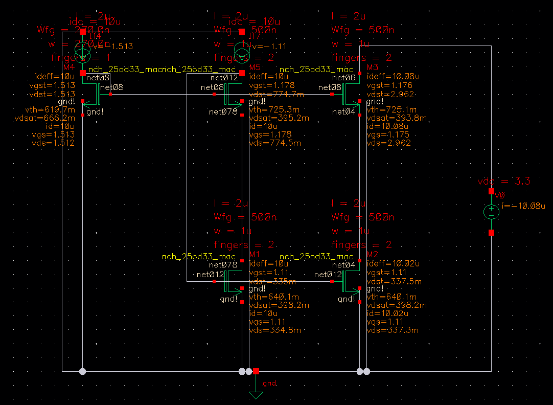
Here is the result of DC simulation of our TSMC 22nm circuit:
  • And this is called “High Swing Cascode” current mirror


Or a little bit different rearranged the same schematic:
Also we could use the same circuit with half a current value of the current referance(s): 5uA and burn less power :
 © 2011-2020 ASIC Stoic. All rights reserved.