In one of the previous blog entries http://asicstoic.blogspot.fr/2015/04/analog-design-basics-nmos.html it is introduced a typical example of an NMOS transistor usage: a current mirror.

Here is example how to size NMOS transistors used in a current mirror copying a desired current.
Foundation of a current mirror design is the fact that:
- two identical transistors are used: meaning both have identical characteristics: VT , Kn, λ and W/L ratios
- both transistors are in saturation mode, sharing the same Vgs
e.g. Because the gate currents are zero for the MOSFETs, reference current IREF must flow into the drain of M1, which is forced to operate in saturation (pinch-off) by the circuit connection
( VDS1 = VGS1 )
- consequently both transistors carry an identical Ids current
e.g. A reference current IREF goes through “diode-connected” transistor M1, establishing gate-source voltage VGS. The same VGS is applied to transistor M2, developing an identical drain current ID2 = Iout= IREF.
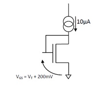
Let’s assume that desired Iref = 10μA.
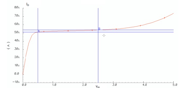
Here is also Id/Vds characteristic of the NMOS transistor used and it can be safely assumed that the transistor is saturated if Vgs = Vt + 200mv.
The transistors are in saturation mode so relation of Id and Vgs is:
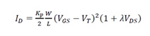
λ is often assumed as 0

© 2011 ASIC Stoic. All rights reserved.
No comments:
Post a Comment