Wednesday, March 18, 2020

Verilog AMS: DUT and testbench code example: Voltage deadband amplifier using Cadence xrun

Verilog AMS: DUT and testbench code example: Voltage deadband amplifier using Cadence xrun


Here is an example of a simple Verilog AMS DUT ( Design Under Test ) of Voltage deadband amplifier ( from my previous post Verilog AMS: Code examples) with its simple Verilog AMS testbench infrastructure.


Also here  is included all files necessary to run the simulation using Cadence xrun command and an example of a possible file directory structure for developing potentialy  multiple Verilog AMS DUT’s
and their respective tests/testbenches.


The files directory structure consists of the following directories :


  • DUT_VAMS:  where all Verilog AMS DUT’s are kept and in this case there is only one, Voltage deadband amplifier:
    • DUT_VAMS/vdba.vams 


  • TESTBENCH: where all verification infrastructure files are kept including:
    • Cadence files necessary to run xrun command, the files that could be shared with multiple Verilog AMS DUT’s and their respective tests/testbenches,  such as: 


      • TESTBENCH/cds_globals.vams:
        `include "disciplines.vams"

        module cds_globals; 
// Global Signals electrical \gnd! ;
ground \gnd! ; wire \vdd! ;
// Design Variables dynamicparam real VDD = 1.8;

endmodule


      • TESTBENCH/probe.tcl:


# define the database for the waveforms database -open waves -into waves.shm -default # probe all probe -create -database waves -all -depth all # run simulation run 1s


    •  TESTBENCH/amscf.scs:

// **************************************************************** // AMS simulation control file for xrun netlist based flow // **************************************************************** simulator lang=spectre // global signals global 0 vdd! // model deck // ams configuration options amsd{ // set the connect rule power supply ie vsup=1.8 } // run a little bit beyond 1s so that simvision // will be active after 1s of transient simulation tran tran stop=1.1 annotate=status


    • A simple Voltage deadband amplifier test/testbench:
      • TESTBENCH/top_vol_deadb_amp.vams 


  • VERIFICATION: Verilog AMS simulation of the DUT is run from here, with a simulation script like this:
    • VERIFICATION/SCRIPTS/run_simulation_voltage_deadband_amplifier
      • Needless to say, the directory VERIFICATION/SCRIPTS could contain all “run simulation” scripts for all DUT’s and in this case it is a home of a “run simulation” script of Voltage deadband
amplifier simple verification script: run_simulation_voltage_deadband_amplifier.tcl:

#!/bin/bash
# run_simulation_voltage_deadband_amplifier.tcl
export DUT_VAMS=./../DUT_VAMS/ export TESTBENCH=./../TESTBENCH/ xrun \ $DUT_VAMS/vdba.vams \ $TESTBENCH/top_vol_deadb_amp.vams \ $TESTBENCH/cds_globals.vams \ $TESTBENCH/amscf.scs \ -timescale 1ns/1ns \ -iereport \ -access +rwc \ -input $TESTBENCH/probe.tcl \ -gui


Here is a summary of all the files and their respective directories in this example (all the files are included in this post Verilog_AMS_VDBA.zip ):


./TESTBENCH/cds_globals.vams
./TESTBENCH/probe.tcl
./TESTBENCH/amscf.scs
./TESTBENCH/top_vol_deadb_amp.vams
./VERIFICATION/clean
./VERIFICATION/SCRIPTS/run_simulation_voltage_deadband_amplifier
./DUT_VAMS/vdba.vams


Verilog AMS implementation  DUT of Voltage deadband amplifier is very simple: the amplifier will “amplify” input voltage signal with the gain of 1, for any voltage except in a “deadband” between 1 -2 V:


// vdba.vams
`include "disciplines.vams"
`timescale 1ns / 1ns 
module vdba(in, out);
input in ;
output out ;
electrical in, out ;


parameter real vin_low =  1.0 ; 
parameter real vin_high = 2.0 ;
parameter real gain = 1 from (0:inf) ;


analog begin
if (V(in) >= vin_high) begin
        
  V(out) <+ gain* V(in)             ;
end
else if (V(in) <= vin_low) begin
  V(out) <+ gain* V(in)            ;
end
else begin
V(out) <+ 0 ;
end
end


endmodule


Verilog AMS implementation of a simple ( not self-checking ) Voltage deadband amplifier  test/testbench of the DUT do a following:  
  • increments DUTs  input voltage every 1 ns for 0.1V until it reaches 5V:


// top_vol_deadb_amp.vams
`include "disciplines.vams"
`timescale 1ns / 1ns 


module top_deadb_amp;
  electrical vin ;
  real d_vin;
  electrical vout;


initial begin


        d_vin = 0;
end


always begin
        #1;
if ( d_vin <= 5 )
d_vin = d_vin + 0.1 ;
else
$finish ;
end    


analog begin

   V(vin) <+ d_vin ;   
  
end


 vdba vdba (
       .in  ( vin  ) , 
       .out ( vout )
);


endmodule


To execute the simulation just do this:
  • cd  <local path>/VERIFICATION
  • ./SCRIPTS/run_simulation_voltage_deadband_amplifier


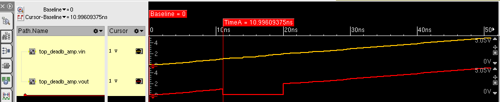
In a  waveforms, here is a result of simulation: 
  • while input is incrementing between 0 and 5V , output is following it except “deadband” in the range of 1-2V when the output is 0V:


© 2011-2019 ASIC Stoic. All rights reserved

Thursday, December 12, 2019

Cadence Virtuoso CMOS Analog Design Basics in TSMC 22nm: A TWO STAGE OPAMP

In the previous blog post “Cadence Virtuoso CMOS Analog Design Basics in TSMC 22nm: a simple op-amp design with a High Swing Cascode current mirror” we fished design of  a simple opamp ( a single stage only ) that reused our High Swing Cascode current mirror.
.


In this blog post we will finally design  A TWO STAGE OPAMP that will reuse our High Swing Cascode current mirror.


A design of  A TWO STAGE OPAMP is very well explained by  Hafeez KT, in his youtube lecture available online and here is a basic topology:


A summary of specification points that will be achieved in this opamp design:

  • our op amp has to drive capacitive load of C1 = 2pF with a 
  • Slew Ratio ( SR ) = 20V/ u second
  • Input Common Mode Range ( negative, minimum ):  ICMR- = 1.2V
    • Voltage on differential pair inputs should never be less than  1.2V
  • Input Common Mode Range ( positive, maximum  ): ICMR+ = 3.0V 
    • Voltage on differential pair inputs should never  not exceed 3.0V
  • Gain Bandwidth product  GBW=30MHZ 


  • DC gain= 1000 ( 60dB )
  • Phase Margin = 60 degrees ( in any case PM should always be bigger than 45 degree )
  • Power < 300uW


Note* : L=1u is used for all transistors.
Assumptions
  • Since this is a two poles and one zero system and to be stable the following condition should be satisfied :
Zero >= 10 * GBW
It can proven, for this topology, that:
  • Cc >= 0.22*CL
=> Cc >= 0.44pF
And a chosen value for Cc in this opamp design is Cc=800fF

Calculation the value of current to be provided by M5 

A friendly reminder that our op amp has to have:
  • Compensation capacitance  Cc = 800fF with a 
  • Slew Ratio ( SR ) = 20V/u second


Fact*: SR is rate of changing voltage across load capacitance Cc


It can be proven 
Q = Cc * V
dQ/dt = Cc*dV/dt
I capacitance = Cc*dV/dt
Cc is charging when differential pair branch M1/M3 is conducting (  and consequently in that case a branch M4/M2 is not conducting ) with the current ID5.
Cc is discharging when differential pair branch M4/M2 is conducting ( consequently branch M1/M3 is not conducting ) with the current ID5.
Conclusion I of capacitance is:
=> I = Cc*dV/dt
=> I = Cc*SR
=> I = 800fF * 20V/ u second = 16uA
=> And a chosen value for I0 or ID5 for this opamp design is:  
I0 or ID5 = 20uA


  • Food for thought: What will happen if every other parameter in the circuit stays constant and only ID5=20uA increases.
=> ID5 increases, transistor “ON” resistance is decreasing because:
And since the gain of the first stage of our opamp is gm1(r01 || r03) 
=> ID5 increases, r0 decreases and overall opamp gain decreases
  • Moral of the story: if required opamp to design has to have high gain don’t start with high value of the biasing current.


In the previous blog we calculated for the PMOS transistor used here :  = 7.85*( 10 ^^ -5 )
       Vth_p    = 603.8mV


Also in the previous blog we calculated we calculated for the NMOS transistor used here  : n*Cox= 649.2*( 10 ^^ -6 )
     Vth_n = 672mV 


Calculation of  W/L for M3/M4 ( pmos active load ) 

A friendly reminder of a point in specification:
  • Input Common Mode Range ( positive, maximum  ) , ICMR+ = 3.0V
    • Voltage on differential pair inputs should never  not exceed 3.0V


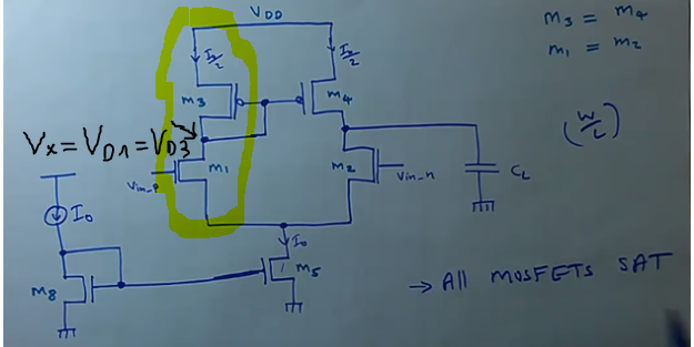
For calculation of  W/L for M3/M4 ( pmos active load ) let’s focus on highlighted transistors M1/M2:


For transistor M0 to be in saturation it is necessary that: VDS3 > VGS3 -Vth_p and ID1=ID3 = 10uA
if Vx = VD1 = VD3 and VDS1 > VGS1 - Vth_n => VD1 > VG1 - Vth_n
=> Vx > Vin_p -Vth_n or
=>  Vin_p < VD1 + Vth_n
It can be proven that:
Using simulation on topology like the one below we found:
=> Vt3 max = 610uV, Vt1min = 700uV
A friendly reminder: = 7.85*( 10 ^^ -5 )
=> (W/L)3 = 1.675 approx. 2
  • Vin min = ICMR- =1.2V


  • Vin max = ICMR+ =3.0V
Food for thought: M3 and M4 transistors are controlling maximum common

mode input range.  It would be logical to make M3 and M4 transistor big to

increase maximum common mode input range. But there is a catch: big M3

and M4 would have smaller “ON” resistance and that would decrease overall

gain of the opamp.


Calculation of  W/L for M1/M2 ( nmos diff. pair ) 


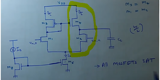
For calculation of  W/L for M1/M2 ( nmos differential pair ) let’s focus on highlighted transistors M4/M2:


A friendly reminder of a couple specification points of our opamp::  
  • Gain Bandwidth product ( GB  = 30MHz )


We will use formula ( and it can be proven that )  GB= DC gain * (first) pole
It can be proven that: 


=> gm1= 30MHz *800fF*2*3.14 = 151u
Because M2= M1 => gm2 = gm1
And finally a chosen value of gm1 = gm2 for design of this opamp is:  
gm2 = gm1= 160u


Finally to calculate M1,2 W/L we will use a formula gm=f(ID, W/L):


A friendly reminder: 
  • n*Cox= 649.2*( 10 ^^ -6 )
  • ID=10uA 


=>  W/L ( for NMOS M1 and M2 ) =  1.97 approx 2 
Food for thought: Transistors M1 and M2 are major contributors to gain and

bandwidth  of the underlined opamp so if you want to design an opamp with a

high gain and high bandwidth then  design high gm of M1 and M2.


Design sizing of M6 transistor

A friendly reminder :
Zero >= 10 * GBW
=> 
  1. Previously calculated: gm2 = gm1= 160u
=> gm6 = 1.6m
It can be proven in this topology that:
and


Now we need to calculate gm4 using formula:
A friendly reminder:
  • ( W/L )4 = 2
  • = 7.85*( 10 ^^ -5 )
  • ID3/4 = 10uA
=> gm3=gm4 = 56u
=>(W/L)6 = 2*(1.6e-3/56e-6)= aprox. 58
Calculation of current through M6
A friendly reminder:
  • (W/L)6  = 58
  • (W/L)4  = 2
=> I6 = 10uA*58/2
=> I6=290uA

Fully transistor sized schematic ( but no current source implemented  yet )


Finally our ( fully sized transistors )  schematic ( after DC simulation with annotated DC operating points ) including:
  • Vdd = 3.3V
  • Vin = 1.2V
Now let’s check our specification requirements:
  1. DC gain should be at least 1000 ( 60dB) and our simulation shows 74.4dB.


  1. GBW should be 30MHz, the current result: 25.357MHz
Calculated values:
gm2 = gm1= 160u
gm3=gm4  = 56u
gm6           = 1.6m


Current simulated values:
gm2 = gm1= 79.55u
gm3=gm4  = 42.74
gm6           = 1.24m

The cause for a low GBW is a low gm1=gm2 so by increasing W/L of M1 and M2 to W/L(1,2)=16 ( and gm1,2 became 170u ) GBW became 30MHz ( Vin common mode is 1.2V ):


Another useful check is to, in DC simulation,  “sweep” Vin from 0V to
3.3V ( VDD ) and to check that for  the range of valid Vin voltages (
ICMR- = 1.2V, ICMR+ = 3.0V )  all 5 transistors are in saturation: 


  1. Phase Margin >= 60 degrees and in simulation it is close enough: 57.81 degrees


4.. Power  <= 300uW while in our calculation it is: 3.3V*(20u+290u) = 102uW


Adding current sources

First I added 20uA sink from High Swing Cascode design from a previous blog post.


There are no significant changes to all measured specification points ( DC gain, GBW and Phase difference ):


Also we will do again of  useful check in DC simulation,  to “sweep” Vin
from 0V to 3.3V ( VDD ) and to check that for  the range of valid Vin
voltages ( ICMR- = 1.2V, ICMR+ = 3.0V )  all 5 transistors are in
saturation: 

Fully transistor sized schematic

Now we are replacing the ideal current source with High Swing Cascode current mirror with added one more current sink of 290uA:


So final schematic looks like this:
Also we will do again of  useful check in DC simulation,  to “sweep” Vin
from 0V to 3.3V ( VDD ) and to check that for  the range of valid Vin
voltages ( ICMR- = 1.2V, ICMR+ = 3.0V )  all 5 transistors are in
saturation: 
And finally to check specification points now when all current sources are added:
  1. DC gain should be at least 1000 ( 60dB) and our simulation shows 74.4 dB.


  1. GBW should be 30MHz, and the current simulation  result is : 25.357MHz


  1. Phase Margin >= 60 degrees and in simulation it is  62.3 degrees
Further increase of (W/L)1,2 from 16 to 24 will do final adjustment of GBW to 30MHz.
As a sanity check lets increase input common mode voltage to its maximum of 3V and check again points of specification:
Also we will do again of  useful check in DC simulation,  to “sweep” Vin
from 0V to 3.3V ( VDD ) and to check that for  the range of valid Vin
voltages ( ICMR- = 1.2V, ICMR+ = 3.0V )  all 5 transistors are in
saturation:

© 2019 ASIC Stoic. All rights reserved