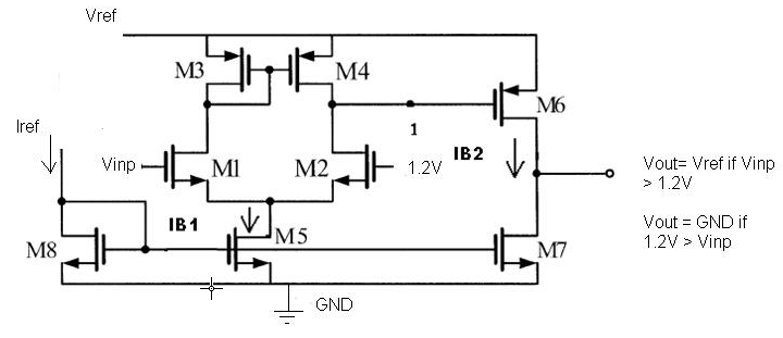
Resistor, Capacitor, Inductor, RLC Circuit, Voltage and Current Sources, A Simple Circuit, Relay Digitally controlled Relay, Comparator, Simple 16-bit digital-to-analog converter model, Simple DAC ( digital input async. or no clock involved),DAC ( digital input async. or no clock involved, but with reference voltage), Simple DAC ( digital input sync. on clock ), Analog tristate buffer, Voltage deadband amplifier, Hysteresis
Code examples
Resistor
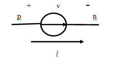
In general, a resistor is a relationship between voltage and current, as in
v = ri
where v represents the voltage across the resistor, i represents the current through the
resistor and r is value of resistance of resistor.
v = V(p,n)
i = I(p,n)
v = ri
module resistor (p, n);
inout p, n;
electrical p, n;
parameter real R = 1.0;
analog
V(p,n) <+ R * I(p,n);
endmodule
Capacitor
A capacitor is a relationship between voltage and charge, as in where v represents the voltage across the capacitor, q represents the charge through the capacitor and c is capacitance of capacitor:
q = cv
Capacitors current is related to its charge like this:
i = dq/dt
So for a linear capacitor, current is:
i = c dv/dt
which is encoded as a Verilog-A/MS contribution statement as
I(p,n) <+ c * ddt(V(p,n));
 // Linear capacitor
module capacitor (p, n);
parameter real c=0; // capacitance (F)
inout p, n;
electrical p, n;
analog
I(p,n) <+ c * ddt(V(p,n));
endmodule
Inductor
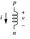
An inductor is a relationship between flux and current, where Φ represents the flux across the inductor, i represents the current through the inductor, and l is inductance of inductor.
Φ = li
flux is related to the voltage using:
v = dΦ/dt
the constitutive relation between inductance, voltage and current is:
v = l di /dt
 // Linear inductor
module inductor(p, n);
parameter real I=0; // inductance (H)
inout p, n;
electrical p, n;
analog
V(p,n) <+ I * ddt(l(p,n));
endmodule
RLC Circuit
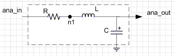 module rlc_behav(ana_in, ana_out) ;
inout ana_in, ana_out ;
electrical ana_in, ana_out ;
parameter real R=1, L=1, C=1 ;
electrical n1 ;
analog begin
V(ana_in, n1) <+ R*I(ana_in, n1) ;
V(n1, ana_out) <+ L*ddt(I(n1, ana_out)) ;
I(ana_out) <+ C*ddt(V(ana_out)) ;
end
endmodule
Voltage and Current Sources
Constant voltage source
// DC voltage source
module vsrc (p, n);
parameter real dc=0; // dc voltage (V)
output p, n;
electrical p, n;
analog
V(p,n) <+ dc;
endmodule
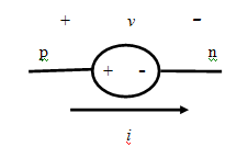
Constant current source
// DC current source
module isrc (p, n);
parameter real dc=0; // dc current (A)
output p, n;
electrical p, n;
analog
l(p,n) <+ dc;
endmodule
A Simple Circuit
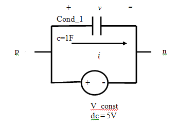 //A simple circuit
`include “V_const.vams”
`include “condensator.vams”
module smpl_ckt;
electrical p,n;
V_const #(.dc(1)) V_const (p,n);
condensator #(.c(1F)) Cond-1 (p,n);
endmodule
Relay
A relay is a switch controlled by analog input (ana_inp),ideal in the sense that when the relay is closed ( ana_inp > treshold ), there is no voltage on its output (ana_out), and when it is open( ana_inp < treshold ) there is no current flowing though its ana_out output contact.
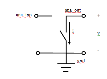 Verilog-A/MS model for an ideal relay.
// Ideal relay
`include “disciplines.vams”
module relay (ana_in, ana_out);
parameter real treshold =0;
output ana_out;
input ana_in;
electrical ana_out, ana_in;
ground gnd ;
analog begin
@(cross( V(ana_in) – treshold , 0 ))
;
if (V(ana_in) > thresh)
V(ana_out) <+ 0;
else
l(ana_out) <+ 0;
end
endmodule
Digitally controlled Relay
module switch (p, n, s);
input s;
output p, n;
logic s;
electrical p, n;
analog begin
if (s)
V(p, n) <+ 0.0;
else
l(p, n) <+ 0.0;
end
endmodule
Comparator
The input of this module is an analog input ( ana_inp ) and the output is a logic signal ( dig_out ).
The output changes when the ana_inp crosses a certain voltage threshold, described as absolute value of parameter offset and parameter hysteresis. The parameter hysteresis provides the capability to add a hysteresis between the lower and the upper thresholds.
// Comparator with logic output
module comparator ( dig_out, ana_inp );
parameter real offset = 0;
parameter real hysteresis = 0.0 from [0:inf);
inout ana_inp;
output dig_out;
electrical ana_inp;
logic dig_out;
reg dig_out;
ground gnd ;
parameter real thrlo = offset – 0.5*hyst; // Lower threshold voltage (V)
parameter real thrhi = offset + 0.5*hyst; // Upper threshold voltage (V)
always @(above(V(ana_inp) – thrhi))
dig_out = 1;
always @(above(thrlo – V(ana_inp)))
dig_out = 0;
endmodule
Simple 16-bit digital-to-analog converter
analog process is sensitive to the value of in at all times
Simple DAC ( digital input async. or no clock involved)
e.g. module dac (out, in);
parameter fullscale = 1.0;
input [15:0] in;
electrical out;
analog
V(out) <+ in * (fullscale/65536);
endmodule
Simple DAC ( digital input sync. on clock )
analog process is only sensitive to the value of in at the instant of a rising edge on clk
module dac (out, in, clk);
parameter fullscale = 1.0;
input [15:0] in;
input clk;
electrical out;
real smpld;
analog begin
@(posedge clk)
smpld = in * (fullscale/65536);
V(out) <+ smpld;
end
endmodule
Analog tristate buffer
This module evaluates the case statement whenever in changes and will set the local
variable value to 0 if in is 0 and to 1 if in is 1. Otherwise it leaves value unchanged.
Finally, it tests the value of in and if not z it drives V(out) with value, otherwise it
leaves out un-driven.
module buf3 (out, in);
input in;
output out;
electrical out;
real value;
analog begin
@(in)
case (in)
1'b0: value = 0;
1'b1: value = 1;
endcase
if (in !== 1'bz)
V(out) <+ value;
end
endmodule
Voltage deadband amplifier
If the input voltage is greater than vin_high or less than vin_low, the amplifier is active.
When the amplifier is active, the output is gain times the differential voltage between the input voltage and the edge of the deadband.
When the input is in the deadband between vin_low and
vin_high, the amplifier is quiescent and the output voltage is zero.
module vdba(in, out);
input in ;
output out ;
electrical in, out ;
parameter real vin_low = -2.0 ;
parameter real vin_high = 2.0 ;
parameter real gain = 1 from (0:inf) ;
analog begin
if (V(in) >= vin_high) begin
V(out) <+ gain*(V(in) - vin_high) ;
end
else if (V(in) <= vin_low) begin
V(out) <+ gain*(V(in) - vin_low) ;
end
else begin
V(out) <+ 0 ;
end
end
endmodule
Hysteresis
 //--------------------
// hysteresis
//
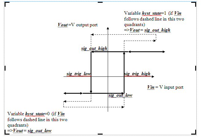
// - rectangular hysteresis
//
module hysteresis(Vin, Vout);
input Vin ;
output Vout;
electrical Vin, Vout;
parameter integer hyst_state_init=1;
parameter real Vout_high = 1 ;
parameter real Vout_low = -1;
parameter real Vout_high = 1 ;
parameter real Vout_low = -1;
integer hyst_state;
real Vout_val;
analog begin
@ ( initial_step ) begin
hyst_state = hyst_state_init;
end
@ (cross (V(Vin) - Vout_high,1) )
if (hyst_state == 0)
hyst_state = 1;
@ (cross (V(Vin) - Vout_low,-1) )
if (hyst_state == 1)
hyst_state = 0;
if (hyst_state == 1) begin
Vout_val = Vout_high;
end
else begin
Vout_val = Vout_low;
end
V(Vout) <+ transition (Vout_val);
end
endmodule
© 2011 ASIC Stoic. All rights reserved.