Thursday, April 2, 2020

Successive Approximation Register (SAR) ADC algorithm - an example


 The SAR ADC is one of the most intuitive analog-to-digital converter algorithm and it can be implemented as a mix design circuit consisting of analog and digital part.

Let's imagine that we need to digitize an analog input signal in the range of 0-1V and that digital samples of the input signals will be represented as 8-bits values.
  • This means that a digital representation of continues analog signal in the range of 0-1V has to be represented with only 2^^8 (256) different values. Foe example: 
    • 0V is represented with a minimum 8 bit value decimal 0 or in binary 8'b0000_0000 and 
    • 1V is represented with maximum 8'bit value decimal 255 or in binary 8'b1111_1111
Since we have only 256 possible digital 8-bit values to represent continues analog signal in the range of 0-1V obviously we will  represent a sub-range of an input voltage with a single 8-bit value.This subrange/step size of the converter defines the converter's resolution.

e.g. 
  • 8'b0000_0000 digital value represents 0V analog input and first next digital value is 8'b0000_0001 that will represent 1V/255 = 0.003922 V if we assume precision on 6 decimal places ( meaning 0.003922 V is the resolution of our ADC in this example ) 
    • This means that we have to adopt a criteria that any input voltage, in the range bigger or equal to 0V and less than 0.003922, will be digitally coded with a value of 8'b0000_0000.
      • Further,  any input voltage in the range bigger or equal of 0.003922 but less than 0.007843( represents result of  2/255)  it will be digitally coded with a value of 8'b0000_0001 etc. etc. 
=> The final table looks like this:
  • There will be 256 ( for example 0, 1, 2....253, 254, 255 ), 8-bit  digital values  representation of the analog input in the range of 0-1V : 
Decimal digital value
Binary digital value
Input analog voltage [V]
Comment
        0
8'b0000_0000
0           
0 /255     = 0             V
        1
8'b0000_0001
0.003922
1 /255     = 0.003922 V  
        2
8'b0000_0010
0.007843 
2 /255     = 0.007843 V
        3
8'b0000_0011
0.011765 
3 /255     = 0.011765 V
.....
…..
…..
…..
        253
8'b1111_1101
0.988235 
253 /255 = 0.988235 V
        254
8'b1111_1110
0.996078 
254 /255 = 0.996078 V
        255
8'b1111_1111
1             
255 /255    = 1           V

And finaly Successive Approximation Register ADC algorithm to output for example a digital value 8'b0000_0001 when input signal is 0.003922 V looks like this:

1.    if  0.003922 V would be bigger or equal than 0.5 V ( this is maximum analog signal voltage of 1V divided by 2 ) MSB bit ( or bit 7)  of a digitized result would be 1 ( but that is not the case so result is 0 )
=> so far the digital result is: 8'b0xxx_xxxx

2.    if  0.003922 V would be bigger or equal than  0.25 V ( this is maximum analog signal voltage of 1V divided by 4 ) bit 6  of a digitized result would be 1 ( but that is not the case so result is 0 )
=> so far the digital result is: 8'b00xx_xxxx

3.    if  0.003922 V would be bigger or equal than  0.125 V ( this is maximum analog signal voltage of 1V divided by 8 ) bit 5  of a digitized result would be 1 ( but that is not the case so result is 0 )
=> so far the digital result is: 8'b000x_xxxx
4.    if  0.003922 V would be bigger or equal than 0.0625  V ( this is maximum analog signal voltage of 1V divided by 16 ) bit 4  of a digitized result would be 1 ( but that is not the case so result is 0 )
=> so far the digital result is: 8'b0000_xxxx
5.    if  0.003922 V would be bigger or equal than  0.03125 V ( this is maximum analog signal voltage of 1V divided by 32 ) bit 3  of a digitized result would be 1 ( but that is not the case so result is 0 ) 
=> so far the digital result is: 8'b0000_0xxx
6.    if  0.003922 V would be bigger or equal than  0.015625 V ( this is maximum analog signal voltage of 1V divided by 64 ) bit 2  of a digitized result would be 1 ( but that is not the case so result is 0 ) 
=> so far the digital result is: 8'b0000_00xx
7.    if  0.003922 V would be bigger or equal than  0.0078125 V ( this is maximum analog signal voltage of 1V divided by 128 ) bit 1  of a digitized result would be 1 ( but that is not the case so result is 0 )
=> so far the digital result is: 8'b0000_000x
8.    if  0.003922 V would be bigger or equal than  0.00390625 V ( this is maximum analog signal voltage of 1V divided by 256 ) LSB bit or bit 0  of a digitized result would be 1, which is the case.
=> and the final result is: 8'b0000_0001

© 2011-2020 ASIC Stoic. All rights reserved

Wednesday, March 18, 2020

Verilog AMS: DUT and testbench code example: Voltage deadband amplifier using Cadence xrun

Verilog AMS: DUT and testbench code example: Voltage deadband amplifier using Cadence xrun


Here is an example of a simple Verilog AMS DUT ( Design Under Test ) of Voltage deadband amplifier ( from my previous post Verilog AMS: Code examples) with its simple Verilog AMS testbench infrastructure.


Also here  is included all files necessary to run the simulation using Cadence xrun command and an example of a possible file directory structure for developing potentialy  multiple Verilog AMS DUT’s
and their respective tests/testbenches.


The files directory structure consists of the following directories :


  • DUT_VAMS:  where all Verilog AMS DUT’s are kept and in this case there is only one, Voltage deadband amplifier:
    • DUT_VAMS/vdba.vams 


  • TESTBENCH: where all verification infrastructure files are kept including:
    • Cadence files necessary to run xrun command, the files that could be shared with multiple Verilog AMS DUT’s and their respective tests/testbenches,  such as: 


      • TESTBENCH/cds_globals.vams:
        `include "disciplines.vams"

        module cds_globals; 
// Global Signals electrical \gnd! ;
ground \gnd! ; wire \vdd! ;
// Design Variables dynamicparam real VDD = 1.8;

endmodule


      • TESTBENCH/probe.tcl:


# define the database for the waveforms database -open waves -into waves.shm -default # probe all probe -create -database waves -all -depth all # run simulation run 1s


    •  TESTBENCH/amscf.scs:

// **************************************************************** // AMS simulation control file for xrun netlist based flow // **************************************************************** simulator lang=spectre // global signals global 0 vdd! // model deck // ams configuration options amsd{ // set the connect rule power supply ie vsup=1.8 } // run a little bit beyond 1s so that simvision // will be active after 1s of transient simulation tran tran stop=1.1 annotate=status


    • A simple Voltage deadband amplifier test/testbench:
      • TESTBENCH/top_vol_deadb_amp.vams 


  • VERIFICATION: Verilog AMS simulation of the DUT is run from here, with a simulation script like this:
    • VERIFICATION/SCRIPTS/run_simulation_voltage_deadband_amplifier
      • Needless to say, the directory VERIFICATION/SCRIPTS could contain all “run simulation” scripts for all DUT’s and in this case it is a home of a “run simulation” script of Voltage deadband
amplifier simple verification script: run_simulation_voltage_deadband_amplifier.tcl:

#!/bin/bash
# run_simulation_voltage_deadband_amplifier.tcl
export DUT_VAMS=./../DUT_VAMS/ export TESTBENCH=./../TESTBENCH/ xrun \ $DUT_VAMS/vdba.vams \ $TESTBENCH/top_vol_deadb_amp.vams \ $TESTBENCH/cds_globals.vams \ $TESTBENCH/amscf.scs \ -timescale 1ns/1ns \ -iereport \ -access +rwc \ -input $TESTBENCH/probe.tcl \ -gui


Here is a summary of all the files and their respective directories in this example (all the files are included in this post Verilog_AMS_VDBA.zip ):


./TESTBENCH/cds_globals.vams
./TESTBENCH/probe.tcl
./TESTBENCH/amscf.scs
./TESTBENCH/top_vol_deadb_amp.vams
./VERIFICATION/clean
./VERIFICATION/SCRIPTS/run_simulation_voltage_deadband_amplifier
./DUT_VAMS/vdba.vams


Verilog AMS implementation  DUT of Voltage deadband amplifier is very simple: the amplifier will “amplify” input voltage signal with the gain of 1, for any voltage except in a “deadband” between 1 -2 V:


// vdba.vams
`include "disciplines.vams"
`timescale 1ns / 1ns 
module vdba(in, out);
input in ;
output out ;
electrical in, out ;


parameter real vin_low =  1.0 ; 
parameter real vin_high = 2.0 ;
parameter real gain = 1 from (0:inf) ;


analog begin
if (V(in) >= vin_high) begin
        
  V(out) <+ gain* V(in)             ;
end
else if (V(in) <= vin_low) begin
  V(out) <+ gain* V(in)            ;
end
else begin
V(out) <+ 0 ;
end
end


endmodule


Verilog AMS implementation of a simple ( not self-checking ) Voltage deadband amplifier  test/testbench of the DUT do a following:  
  • increments DUTs  input voltage every 1 ns for 0.1V until it reaches 5V:


// top_vol_deadb_amp.vams
`include "disciplines.vams"
`timescale 1ns / 1ns 


module top_deadb_amp;
  electrical vin ;
  real d_vin;
  electrical vout;


initial begin


        d_vin = 0;
end


always begin
        #1;
if ( d_vin <= 5 )
d_vin = d_vin + 0.1 ;
else
$finish ;
end    


analog begin

   V(vin) <+ d_vin ;   
  
end


 vdba vdba (
       .in  ( vin  ) , 
       .out ( vout )
);


endmodule


To execute the simulation just do this:
  • cd  <local path>/VERIFICATION
  • ./SCRIPTS/run_simulation_voltage_deadband_amplifier


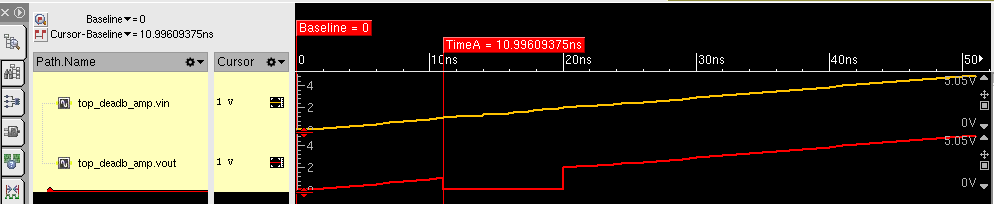
In a  waveforms, here is a result of simulation: 
  • while input is incrementing between 0 and 5V , output is following it except “deadband” in the range of 1-2V when the output is 0V:


© 2011-2019 ASIC Stoic. All rights reserved